- 您現(xiàn)在的位置:買賣IC網(wǎng) > PDF目錄359243 > MVTX2601AG (ZARLINK SEMICONDUCTOR INC) Unmanaged 24-Port 10/100 Mbps Ethernet Switch PDF資料下載
參數(shù)資料
| 型號(hào): | MVTX2601AG |
| 廠商: | ZARLINK SEMICONDUCTOR INC |
| 元件分類: | 網(wǎng)絡(luò)接口 |
| 英文描述: | Unmanaged 24-Port 10/100 Mbps Ethernet Switch |
| 中文描述: | DATACOM, LAN SWITCHING CIRCUIT, PBGA553 |
| 封裝: | 37.50 X 37.50 MM, 2.33 MM HEIGHT, MS-034, HSBGA-553 |
| 文件頁數(shù): | 13/91頁 |
| 文件大小: | 686K |
| 代理商: | MVTX2601AG |
第1頁第2頁第3頁第4頁第5頁第6頁第7頁第8頁第9頁第10頁第11頁第12頁當(dāng)前第13頁第14頁第15頁第16頁第17頁第18頁第19頁第20頁第21頁第22頁第23頁第24頁第25頁第26頁第27頁第28頁第29頁第30頁第31頁第32頁第33頁第34頁第35頁第36頁第37頁第38頁第39頁第40頁第41頁第42頁第43頁第44頁第45頁第46頁第47頁第48頁第49頁第50頁第51頁第52頁第53頁第54頁第55頁第56頁第57頁第58頁第59頁第60頁第61頁第62頁第63頁第64頁第65頁第66頁第67頁第68頁第69頁第70頁第71頁第72頁第73頁第74頁第75頁第76頁第77頁第78頁第79頁第80頁第81頁第82頁第83頁第84頁第85頁第86頁第87頁第88頁第89頁第90頁第91頁

MVTX2601
Data Sheet
13
Zarlink Semiconductor Inc.
3.2 Multicast Data Frame Forwarding
After receiving the switch response, the TxQ manager has to make the dropping decision. A global decision to drop
can be made, based on global FDB utilization and reservations. If so, then the FCB is released and the frame is
dropped. In addition, a selective decision to drop can be made, based on the TxQ occupancy at some subset of the
multicast packet’s destinations. If so, then the frame is dropped at some destinations but not others and the FCB is
not released.
If the frame is not dropped at a particular destination port, then the TxQ manager formats an entry in the multicast
queue for that port and class. Multicast queues are physical queues (unlike the linked lists for unicast frames).
There are 2 multicast queues for each of the 24 10/100 ports. The queue with higher priority has room for 32 entries
and the queue with lower priority has room for 64 entries. There is one multicast queue for every two priority
classes. For the 10/100 ports to map the 8 transmit priorities into 2 multicast queues, the 2 LSB are discarded.
During scheduling, the TxQ manager treats the unicast queue and the multicast queue of the same class as one
logical queue. The older head of line of the two queues is forwarded first.
The port control requests a FCB release only after the EOF for the multicast frame has been read by all ports to
which the frame is destined.
4.0 Memory Interface
4.1 Overview
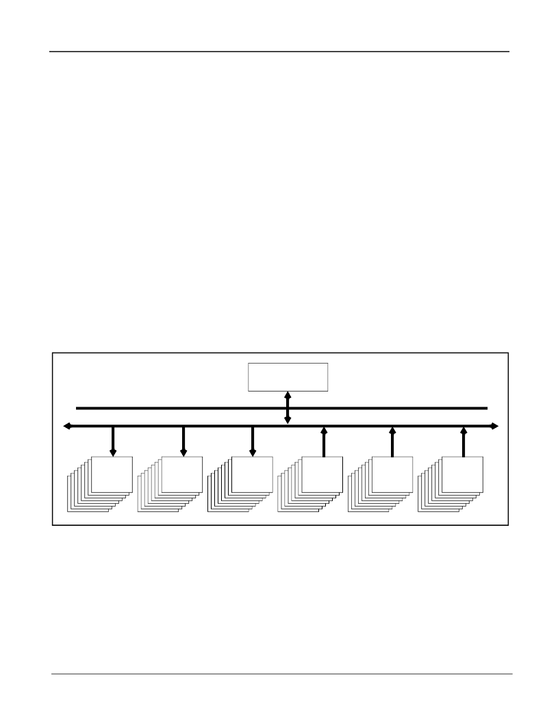
The MVTX2601 provides a 64-bit wide SRAM bank. Each DMA can read and write from the SRAM bank. The
following figure provides an overview of the MVTX2601 SRAM bank.
Figure 3 - MVTX2601 SRAM Interface Block Diagram (DMAs for 10/1000 Ports Only)
4.2 Detailed Memory Information
Because the bus for each bank is 64 bits wide, frames are broken into 8-byte granules, written to and read from
memory.
4.3 Memory Requirements
To support 64 K MAC address, 2 MB memory is required. When VLAN support is enabled, 512 entries of the MAC
address table are used for storing the VLAN ID at VLAN Index Mapping Table.
SRAM
TX DMA
0-7
TX DMA
8-15
TX DMA
16-23
RX DMA
0-7
RX DMA
8-15
RX DMA
16-23
相關(guān)PDF資料 |
PDF描述 |
|---|---|
| MVTX2602 | Managed 24 Port 10/100 Mbps Ethernet Switch |
| MVTX2602AG | Managed 24 Port 10/100 Mbps Ethernet Switch |
| MVTX2603 | Unmanaged 24-Port 10/100 Mb + 2-Port 1 Gb Ethernet Switch |
| MVTX2603AG | Unmanaged 24-Port 10/100 Mb + 2-Port 1 Gb Ethernet Switch |
| MVTX2604 | Managed 24-Port 10/100 Mb + 2 Port 1 Gb Ethernet Switch |
相關(guān)代理商/技術(shù)參數(shù) |
參數(shù)描述 |
|---|---|
| MVTX2601AG2 | 制造商:Microsemi Corporation 功能描述: |
| MVTX2602 | 制造商:ZARLINK 制造商全稱:Zarlink Semiconductor Inc 功能描述:Managed 24 Port 10/100 Mbps Ethernet Switch |
| MVTX2602A | 制造商:未知廠家 制造商全稱:未知廠家 功能描述:MVTX260x Port Mirroring |
| MVTX2602AG | 制造商:ZARLINK 制造商全稱:Zarlink Semiconductor Inc 功能描述:Managed 24 Port 10/100 Mbps Ethernet Switch |
| MVTX2602AG2 | 制造商:Microsemi Corporation 功能描述: |
發(fā)布緊急采購,3分鐘左右您將得到回復(fù)。