- 您現(xiàn)在的位置:買賣IC網(wǎng) > PDF目錄361099 > NCP3063 (ON SEMICONDUCTOR) 500kHz and 1MHz High Efficiency 1.5A Switching Regulators; Package: SO; No of Pins: 8; Temperature Range: -40?°C to 85?°C PDF資料下載
參數(shù)資料
| 型號: | NCP3063 |
| 廠商: | ON SEMICONDUCTOR |
| 元件分類: | 穩(wěn)壓器 |
| 英文描述: | 500kHz and 1MHz High Efficiency 1.5A Switching Regulators; Package: SO; No of Pins: 8; Temperature Range: -40?°C to 85?°C |
| 中文描述: | 1.5 A SWITCHING REGULATOR, 190 kHz SWITCHING FREQ-MAX, DSO8 |
| 封裝: | 4 X 4 MM, LEAD FREE, DFN-8 |
| 文件頁數(shù): | 9/16頁 |
| 文件大小: | 269K |
| 代理商: | NCP3063 |
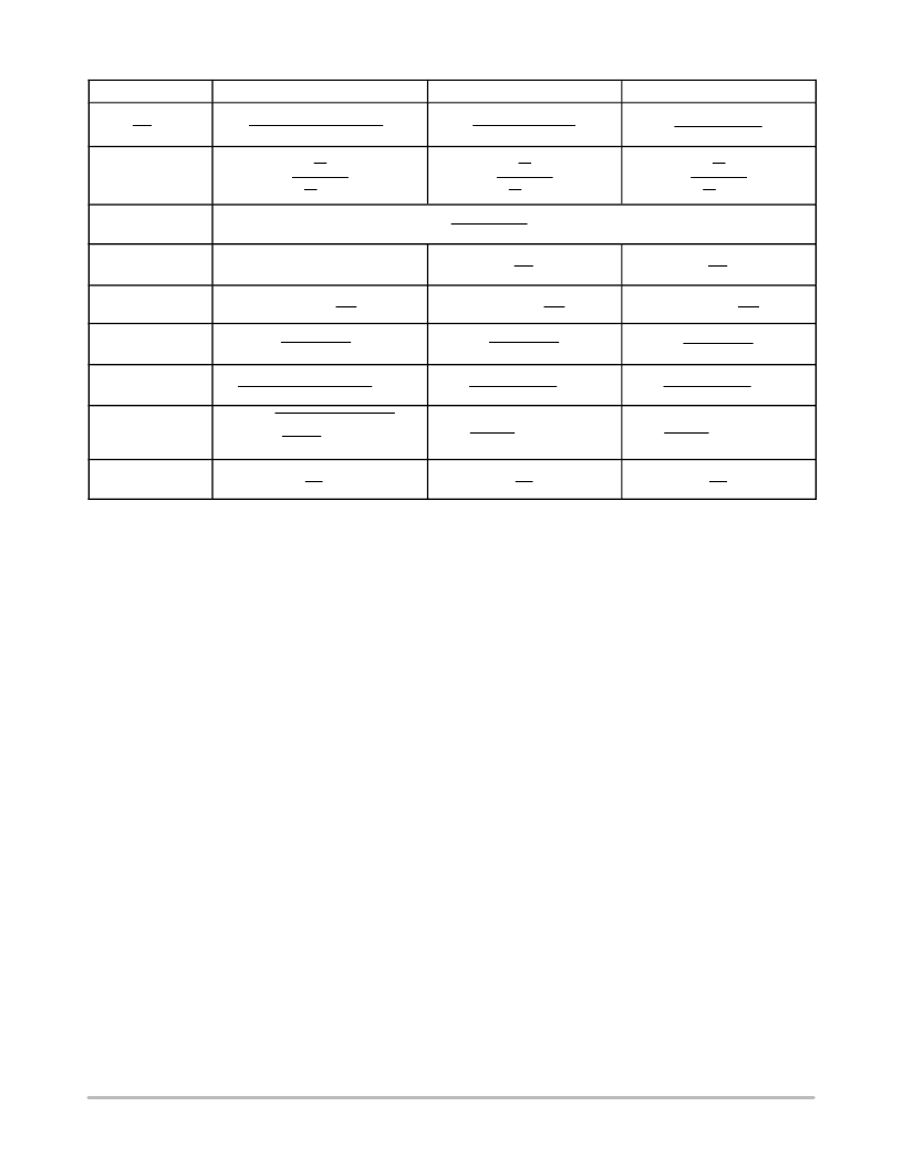
NCP3063, NCP3063B, NCV3063
http://onsemi.com
9
(See Notes 9, 10, 11)
StepDown
StepUp
VoltageInverting
ton
toff
t
on
Vout
VSWCE
VF
Vin
Vout
Vout
Vin
VF
VSWCE
Vin
|Vout|
Vin
VF
VSWCE
ton
toff
f
ton
toff
1
ton
toff
f
ton
toff
1
ton
toff
f
ton
toff
1
C
T
CT
381.6
10
6
fosc
343
10
12
I
L(avg)
Iout
Iout
ton
toff
1
Iout
ton
toff
1
I
pk (Switch)
IL(avg)
IL
2
IL(avg)
IL
2
IL(avg)
IL
2
R
SC
0.20
Ipk (Switch)
0.20
Ipk (Switch)
0.20
Ipk (Switch)
L
Vin
VSWCE
Vout
IL
ton
Vin
VSWCE
IL
ton
Vin
VSWCE
IL
ton
V
ripple(pp)
IL
1
8
f
CO
2
(ESR)
2
tonIout
CO
IL
ESR
tonIout
CO
IL
ESR
V
out
VTH
R2
R1
1
VTH
R2
R1
1
VTH
R2
R1
1
The Following Converter Characteristics Must Be Chosen:
V
in
Nominal operating input voltage.
V
out
Desired output voltage.
I
out
Desired output current.
I
L
Desired peaktopeak inductor ripple current. For maximum output current it is suggested that I
L
be chosen to be
less than 10% of the average inductor current I
L(avg)
. This will help prevent I
pk (Switch)
from reaching the current limit threshold
set by R
SC
. If the design goal is to use a minimum inductance value, let I
L
= 2(I
L(avg)
). This will proportionally reduce
converter output current capability.
f
Maximum output switch frequency.
V
ripple(pp)
Desired peaktopeak output ripple voltage. For best performance the ripple voltage should be kept to a low
value since it will directly affect line and load regulation. Capacitor C
O
should be a low equivalent series resistance (ESR)
electrolytic designed for switching regulator applications.
9. V
SWCE
Darlington Switch Collector to Emitter Voltage Drop, refer to Figures 5, 6, 7 and 8.
10.V
F
Output rectifier forward voltage drop. Typical value for 1N5819 Schottky barrier rectifier is 0.4 V.
11.The calculated t
on
/t
off
must not exceed the minimum guaranteed oscillator charge to discharge ratio.
Figure 13. Design Equations
相關(guān)PDF資料 |
PDF描述 |
|---|---|
| NCP3063B | 500kHz and 1MHz High Efficiency 1.5A Switching Regulators; Package: SO; No of Pins: 8; Temperature Range: -40?°C to 85?°C |
| NCV3063 | 500kHz and 1MHz High Efficiency 1.5A Switching Regulators; Package: SO; No of Pins: 8; Temperature Range: -40?°C to 85?°C |
| NCP345SNT1 | Overvoltage Protection IC |
| NCP1651DR2 | Single Stage Power Factor Controller |
| NCP1651 | Single Stage Power Factor Controller |
相關(guān)代理商/技術(shù)參數(shù) |
參數(shù)描述 |
|---|---|
| NCP3063_Boost_EVB | 制造商:ON Semiconductor 功能描述:1.5 A, Step-Up/Down/Inverting Switching Regulators 制造商:ON Semiconductor 功能描述:BOOST application Development board |
| NCP3063_Buck_EVB | 制造商:ON Semiconductor 功能描述:BUCK application Development board 制造商:ON Semiconductor 功能描述:1.5 A, Step-Up/Down/Inverting Switching Regulators |
| NCP3063_Invert_EVB | 制造商:ON Semiconductor 功能描述:Inverting application Development board 制造商:ON Semiconductor 功能描述:1.5 A, Step-Up/Down/Inverting Switching Regulators |
| NCP3063BDR2G | 功能描述:直流/直流開關(guān)調(diào)節(jié)器 1.5 A DCDC SW REG RoHS:否 制造商:International Rectifier 最大輸入電壓:21 V 開關(guān)頻率:1.5 MHz 輸出電壓:0.5 V to 0.86 V 輸出電流:4 A 輸出端數(shù)量: 最大工作溫度: 安裝風(fēng)格:SMD/SMT 封裝 / 箱體:PQFN 4 x 5 |
| NCP3063BDR2G-CUT TAPE | 制造商:ON 功能描述:NCP3063B Series 40 V 1.5 A Step-Up/Down/ Inverting Switching Regulator - SOIC-8 |
發(fā)布緊急采購,3分鐘左右您將得到回復(fù)。