- 您現(xiàn)在的位置:買賣IC網(wǎng) > PDF目錄361100 > NCP500SQL50T1G (ON SEMICONDUCTOR) 150 mA CMOS Low Noise Low−Dropout Voltage Regulator PDF資料下載
參數(shù)資料
| 型號: | NCP500SQL50T1G |
| 廠商: | ON SEMICONDUCTOR |
| 元件分類: | 基準電壓源/電流源 |
| 英文描述: | 150 mA CMOS Low Noise Low−Dropout Voltage Regulator |
| 中文描述: | 5 V FIXED POSITIVE LDO REGULATOR, 0.18 V DROPOUT, PDSO6 |
| 封裝: | 2 X 2.2 MM, LEAD FREE, DFN-6 |
| 文件頁數(shù): | 2/20頁 |
| 文件大小: | 153K |
| 代理商: | NCP500SQL50T1G |
NCP500
http://onsemi.com
2
ááááááááááááááááááááááááááááááááá
ááááááááááááááááááááááááááááááááá
ááááááááááááááááááááááááááááááááá
ááááááááááááááááááááááááááááááááá
ááááááááááááááááááááááááááááááááá
ááááááááááááááááááááááááááááááááá
ááááááááááááááááááááááááááááááááá
ááááááááááááááááááááááááááááááááá
ááááááááááááááááááááááááááááááááá
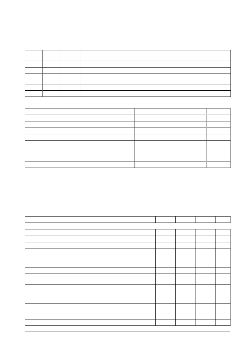
Pin No.
Pin No.
Pin Name
Description
1
3
V
Positive power supply input voltage.
2
2, 5
1
6
GND
Enable
N/C
Power supply ground.
This input is used to place the device into lowpower standby. When this input is pulled to a logic
in
4
No internal connection.
5
4
V
out
Regulated output voltage.
MAXIMUM RATINGS
ááááááááááááááááááááááááááááááááá
ááááááááááááááááááááááááááááááááá
ááááááááááááááááááááááááááááááááá
ááááááááááááááááááááááááááááááááá
ááááááááááááááááááááááááááááááááá
Thermal Resistance, JunctiontoAmbient
TSOP5
DFN (Note 3)
R
JA
in
°
C/W
on/off
in
out
in
250
225
ááááááááááááááááááááááááááááááááá
ááááááááááááááááááááááááááááááááá
ááááááááááááááááááááááááááááááááá
Maximum ratings are those values beyond which device damage can occur. Maximum ratings applied to the device are individual stress limit
values (not normal operating conditions) and are not valid simultaneously. If these limits are exceeded, device functional operation is not implied,
damage may occur and reliability may be affected.
1. This device series contains ESD protection and exceeds the following tests:
Human Body Model 2000 V per MILSTD883, Method 3015
Machine Model Method 200 V
Latch up capability (85
°
C)
2. Device is internally limited to 160
°
C by thermal shutdown.
3. For more information, refer to application note, AND8080/D.
Operating Junction Temperature
T
J
+125
°
C
Storage Temperature
T
stg
65 to +150
°
C
100 mA.
ELECTRICAL CHARACTERISTICS
(V
in
= 2.35 V, C
in
= 1.0 F, C
out
= 1.0 F, for typical value T
A
= 25
°
C, for min and
max values T
A
= 40
°
C to 85
°
C, T
jmax
= 125
°
C, unless otherwise noted)
Characteristic
Symbol
Min
Typ
Max
Unit
1.8 V
Output Voltage (T
A
= 40
°
C to 85
°
C, I
out
= 1.0 mA to 150 mA)
V
out
1.755
1.8
1.845
V
Line Regulation (V
in
= 2.3 V to 6.0 V, I
out
= 1.0 mA)
Reg
line
1.0
10
mV
Load Regulation (I
out
= 1.0 mA to 150 mA)
Reg
load
15
45
mV
Dropout Voltage (Measured at V
out
2.0%, T
A
= 40
°
C to 85
°
C)
(Iout = 1.0 mA)
(Iout = 75 mA)
(Iout = 150 mA)
V
in
V
out
2.0
140
270
10
200
350
mV
Output Short Circuit Current
I
out(max)
200
540
700
mA
Ripple Rejection
(V
in
= V
out (nom.)
+ 1.0 V + 0.5 V
pp
, f = 1.0 kHz, I
o
= 60 mA)
RR
62
dB
Quiescent Current
(Enable Input = 0 V)
(Enable Input = 0.9 V, I
out
= 1.0 mA)
(Enable Input = 0.9 V, I
out
= 150 mA)
I
Q
0.01
175
175
1.0
300
300
A
Enable Input Threshold Voltage
(Voltage Increasing, Output Turns On, Logic High)
(Voltage Decreasing, Output Turns Off, Logic Low)
V
th(EN)
0.9
0.15
V
Enable Input Bias Current
I
IB(EN)
3.0
100
nA
相關PDF資料 |
PDF描述 |
|---|---|
| NCP500SN33T1 | 150 mA CMOS Low Noise Low-Dropout Voltage Regulator |
| NCP500SQL33T1 | 150 mA CMOS Low Noise Low-Dropout Voltage Regulator |
| NCP500D | 150 mA CMOS Low Noise Low-Dropout Voltage Regulator |
| NCP500SN185T1 | 150 mA CMOS Low Noise Low-Dropout Voltage Regulator |
| NCP500SN18T1 | 150 mA CMOS Low Noise Low-Dropout Voltage Regulator |
相關代理商/技術參數(shù) |
參數(shù)描述 |
|---|---|
| NCP5010 | 制造商:ONSEMI 制造商全稱:ON Semiconductor 功能描述:500 mW Boost Converter for White LEDs |
| NCP5010_06 | 制造商:ONSEMI 制造商全稱:ON Semiconductor 功能描述:500 mW Boost Converter for White LEDs |
| NCP5010EVB | 功能描述:電源管理IC開發(fā)工具 EVAL BRD FOR NCP5010FCT1G RoHS:否 制造商:Maxim Integrated 產(chǎn)品:Evaluation Kits 類型:Battery Management 工具用于評估:MAX17710GB 輸入電壓: 輸出電壓:1.8 V |
| NCP5010FCT1G | 功能描述:開關變換器、穩(wěn)壓器與控制器 WHITE LED DRIVER RoHS:否 制造商:Texas Instruments 輸出電壓:1.2 V to 10 V 輸出電流:300 mA 輸出功率: 輸入電壓:3 V to 17 V 開關頻率:1 MHz 工作溫度范圍: 安裝風格:SMD/SMT 封裝 / 箱體:WSON-8 封裝:Reel |
| NCP502 | 制造商:ONSEMI 制造商全稱:ON Semiconductor 功能描述:80 mA CMOS Low Iq Voltage Regulator in an SC70−5 |
發(fā)布緊急采購,3分鐘左右您將得到回復。