- 您現(xiàn)在的位置:買賣IC網(wǎng) > PDF目錄361102 > NCP5318 (ON SEMICONDUCTOR) Two/Three/Four−Phase Buck CPU Controller PDF資料下載
參數(shù)資料
| 型號(hào): | NCP5318 |
| 廠商: | ON SEMICONDUCTOR |
| 英文描述: | Two/Three/Four−Phase Buck CPU Controller |
| 文件頁數(shù): | 24/31頁 |
| 文件大小: | 384K |
| 代理商: | NCP5318 |
第1頁第2頁第3頁第4頁第5頁第6頁第7頁第8頁第9頁第10頁第11頁第12頁第13頁第14頁第15頁第16頁第17頁第18頁第19頁第20頁第21頁第22頁第23頁當(dāng)前第24頁第25頁第26頁第27頁第28頁第29頁第30頁第31頁
NCP5318
http://onsemi.com
24
I
RMS,CNTL
is the RMS value of the current in the control
MOSFET:
IRMS,CNTL
(D
(ILo,MAX2
ILo,MAX
ILo,MIN
(eq. 21)
ILo,MIN2
3
))1 2
I
Lo,MAX
is the maximum output inductor current:
ILo,MAX
IO,MAX
ILo
2
(eq. 22)
I
Lo,MIN
is the minimum output inductor current:
ILo,MIN
IO,MAX
ILo
2
(eq. 23)
I
O,MAX
is the maximum converter output current.
D is the duty cycle of the converter:
D
VOUT
VIN
(eq. 24)
I
Lo
is the peak
to
peak ripple current in the output
inductor of value L
o
:
ILo
(VIN
VOUT)
D
(Lo
fSW)
(eq. 25)
R
DS(on)
is the ON resistance of the high side MOSFET at
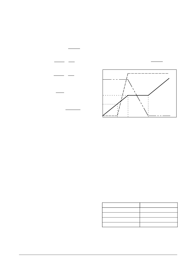
the applied gate drive voltage. Q
switch
is the post gate
threshold portion of the gate
to
source charge plus the
gate
to
drain charge. This may be specified in the data sheet
or approximated from the gate
charge curve as shown in the
Figure 25.
Qswitch
Qgs2
Qgd
(eq. 26)
I
g
is the output current from the gate driver IC.
V
IN
is the input voltage to the converter.
f
sw
is the switching frequency of the converter.
Q
RR
is the reverse recovery charge of the
lower
MOSFET.
Q
oss
is the sum of the high and low side MOSFET
output charges specified in the data sheets, or
estimated from integrating C
OSS
from zero volts to
V
IN
.
For the lower or synchronous MOSFET, the power
dissipation can be approximated from:
(IRMS,SYNCH2
(Vfdiode
IO,MAX
PD,SYNCH
RDS(on))
tnonoverlap
fSW)
(eq. 27)
where:
Vf
diode
is the forward voltage of the MOSFET’s
intrinsic diode at the converter output current.
t
nonoverlap
is the non
overlap time between the upper
and lower gate drivers to prevent cross conduction.
This time is usually specified in the data sheet for the
driver IC.
The first term represents the conduction or I
2
R losses
when the MOSFET is ON and the second term represents the
diode losses that occur during the gate non
overlap time.
All terms were defined in the previous discussion for the
control MOSFET with the exception of:
(eq. 28)
IRMS,SYNCH
(ILo,MAX2
((1
D)
ILo,MAX
ILo,MIN
ILo,MIN2
3
))1 2
I
D
V
GATE
V
DRAIN
Q
GD
Q
GS2
Q
GS1
V
GS_TH
Figure 25. MOSFET Switching Characteristics
When the MOSFET power dissipations are known, the
designer can calculate the required thermal impedance to
maintain a specified junction temperature at the worst case
ambient operating temperature.
T
(TJ
TA) PD
(eq. 29)
where:
T
is the total thermal impedance (
JC
+
SA
);
JC
is the junction
to
case thermal impedance of the
MOSFET;
SA
is the sink
to
ambient thermal impedance of
the heatsink assuming direct mounting of the
MOSFET if no thermal “pad” is used;
T
J
is the specified maximum allowed junction
temperature;
T
A
is the worst case ambient operating temperature.
For TO
220 and TO
263 packages, standard FR
4
copper clad circuit boards will have approximate thermal
resistances (
SA
) as shown below:
Pad Size (in
2
/mm
2
)
Single
Sided 1 oz. Copper
0.50/323
60
65
°
C/W
0.75/484
55
60
°
C/W
1.00/645
50
55
°
C/W
1.50/968
45
50
°
C/W
相關(guān)PDF資料 |
PDF描述 |
|---|---|
| NCP5318FTR2 | Two/Three/Four−Phase Buck CPU Controller |
| NCP5318FTR2G | Two/Three/Four−Phase Buck CPU Controller |
| NCP5322ADWG | Two−Phase Buck Controller with Integrated Gate Drivers and 5−Bit DAC |
| NCP5322ADWR2G | Two−Phase Buck Controller with Integrated Gate Drivers and 5−Bit DAC |
| NCP5331FTR2G | Two-Phase PWM Controller with Integrated Gate Drivers |
相關(guān)代理商/技術(shù)參數(shù) |
參數(shù)描述 |
|---|---|
| NCP5318FTR2 | 功能描述:DC/DC 開關(guān)控制器 2/3/4 Phase Buck CPU RoHS:否 制造商:Texas Instruments 輸入電壓:6 V to 100 V 開關(guān)頻率: 輸出電壓:1.215 V to 80 V 輸出電流:3.5 A 輸出端數(shù)量:1 最大工作溫度:+ 125 C 安裝風(fēng)格: 封裝 / 箱體:CPAK |
| NCP5318FTR2G | 功能描述:DC/DC 開關(guān)控制器 2/3/4 Phase Buck CPU RoHS:否 制造商:Texas Instruments 輸入電壓:6 V to 100 V 開關(guān)頻率: 輸出電壓:1.215 V to 80 V 輸出電流:3.5 A 輸出端數(shù)量:1 最大工作溫度:+ 125 C 安裝風(fēng)格: 封裝 / 箱體:CPAK |
| NCP5322A | 制造商:ONSEMI 制造商全稱:ON Semiconductor 功能描述:Two−Phase Buck Controller with Integrated Gate Drivers and 5−Bit DAC |
| NCP5322A/D | 制造商:ONSEMI 制造商全稱:ON Semiconductor 功能描述:Two-Phase Buck Controller with integrated Gate Drivers and 5-Bit DAC |
| NCP5322A_07 | 制造商:ONSEMI 制造商全稱:ON Semiconductor 功能描述:Two−Phase Buck Controller with Integrated Gate Drivers and 5−Bit DAC |
發(fā)布緊急采購,3分鐘左右您將得到回復(fù)。