- 您現(xiàn)在的位置:買(mǎi)賣(mài)IC網(wǎng) > PDF目錄224620 > OP-37AJG (TEXAS INSTRUMENTS INC) OP-AMP, 60 uV OFFSET-MAX, 63 MHz BAND WIDTH, CDIP8 PDF資料下載
參數(shù)資料
| 型號(hào): | OP-37AJG |
| 廠商: | TEXAS INSTRUMENTS INC |
| 元件分類(lèi): | 運(yùn)算放大器 |
| 英文描述: | OP-AMP, 60 uV OFFSET-MAX, 63 MHz BAND WIDTH, CDIP8 |
| 封裝: | CERAMIC, DIP-8 |
| 文件頁(yè)數(shù): | 1/24頁(yè) |
| 文件大?。?/td> | 391K |
| 代理商: | OP-37AJG |
當(dāng)前第1頁(yè)第2頁(yè)第3頁(yè)第4頁(yè)第5頁(yè)第6頁(yè)第7頁(yè)第8頁(yè)第9頁(yè)第10頁(yè)第11頁(yè)第12頁(yè)第13頁(yè)第14頁(yè)第15頁(yè)第16頁(yè)第17頁(yè)第18頁(yè)第19頁(yè)第20頁(yè)第21頁(yè)第22頁(yè)第23頁(yè)第24頁(yè)
OP27A, OP27C, OP27E, OP27G
OP37A, OP37C, OP37E, OP37G
LOW-NOISE HIGH-SPEED PRECISION OPERATIONAL-AMPLIFIER
SLOS100C – FEBRUARY 1989 – REVISED SEPTEMBER 2000
1
POST OFFICE BOX 655303
DALLAS, TEXAS 75265
D Direct Replacements for PMI and LTC OP27
and OP37 Series
Features of OP27A, OP27C, OP37A, and
OP37C:
D Maximum Equivalent Input Noise Voltage:
3.8 nV/
√Hz at 1 kHz
5.5 nV/
√Hz at 10 kHz
D Very Low Peak-to-Peak Noise Voltage at
0.1 Hz to 10 Hz . . . 80 nV Typ
D Low Input Offset Voltage ...25 V Max
D High Voltage Amplification ...1 V/V Min
Feature of OP37 Series:
D Minimum Slew Rate ...11 V/s
description
The OP27 and OP37 operational amplifiers
combine outstanding noise performance with
excellent precision and high-speed specifica-
tions. The wideband noise is only 3 nV/
√Hz and
with the 1/f noise corner at 2.7 Hz, low noise is
maintained for all low-frequency applications.
The outstanding characteristics of the OP27 and
OP37 make these devices excellent choices
for low-noise amplifier applications requiring
precision performance and reliability. Additionally,
the OP37 is free of latch-up in high-gain,
large-capacitive-feedback configurations.
The OP27 series is compensated for unity gain.
The OP37 series is decompensated for increased
bandwidth and slew rate and is stable down to a
gain of 5.
The OP27A, OP27C, OP37A, and OP37C are characterized for operation over the full military temperature
range of – 55
°C to 125°C. The OP27E, OP27G, OP37E, and OP37G are characterized for operation from – 25°C
to 85
°C.
AVAILABLE OPTIONS
VIOmax
STABLE
PACKAGE
TA
VIOmax
AT 25
°C
STABLE
GAIN
CERAMIC DIP
(JG)
CHIP CARRIER
(FK)
PLASTIC DIP
(P)
25
V
1
—
OP27EP
25
°Cto85°C
25
V
5
—
OP37EP
– 25
°C to 85°C
100
V
1
—
OP27GP
100
V
5
—
OP37GP
25
V
1
OP27AJG
OP27AFK
—
55
°Cto125°C
25
V
5
OP37AJG
OP37AFK
—
– 55
°C to 125°C
100
V
1
OP27CJG
—
100
V
5
OP37CJG
—
Copyright
2000, Texas Instruments Incorporated
PRODUCTION DATA information is current as of publication date.
Products conform to specifications per the terms of Texas Instruments
standard warranty. Production processing does not necessarily include
testing of all parameters.
Please be aware that an important notice concerning availability, standard warranty, and use in critical applications of
Texas Instruments semiconductor products and disclaimers thereto appears at the end of this data sheet.
1
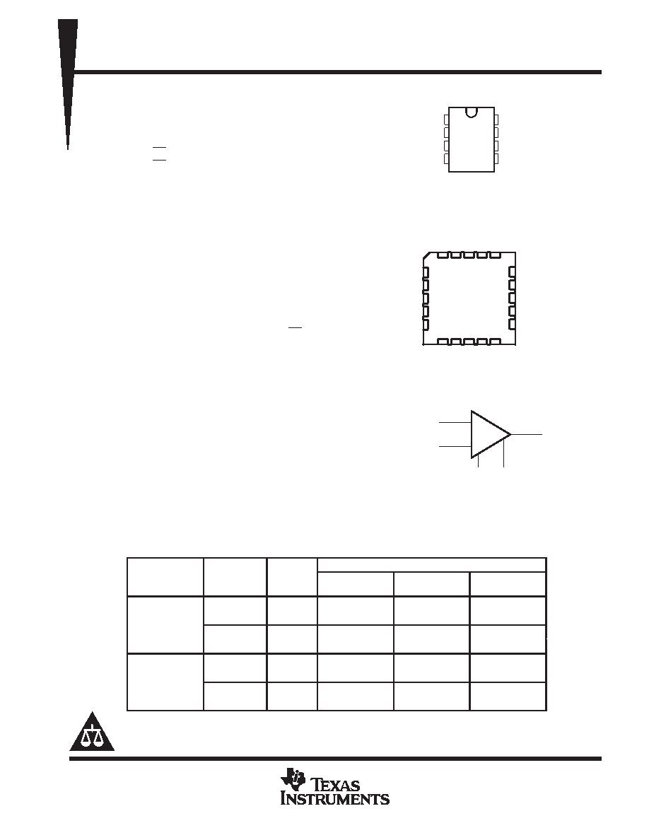
2
3
4
8
7
6
5
VIOTRIM
IN –
IN +
VCC –
VIOTRIM
VCC+
OUT
NC
JG OR P PACKAGE
(TOP VIEW)
IN +
IN –
OUT
VIO TRIM
18
6
3
2
symbol
3
2
1 20 19
910 11 12 13
4
5
6
7
8
18
17
16
15
14
NC
VCC+
NC
OUT
NC
1N –
NC
IN +
NC
FK PACKAGE
(TOP VIEW)
NC
NC – No internal connection
CC
–
V
Pin numbers are for the JG and P packages.
IO
V
TRIM
+
–
NC
IO
V
TRIM
相關(guān)PDF資料 |
PDF描述 |
|---|---|
| OP-37EP | OP-AMP, 60 uV OFFSET-MAX, 63 MHz BAND WIDTH, PDIP8 |
| OP-37CJG | OP-AMP, 300 uV OFFSET-MAX, 63 MHz BAND WIDTH, CDIP8 |
| OP-37GP | OP-AMP, 220 uV OFFSET-MAX, 63 MHz BAND WIDTH, PDIP8 |
| OP-47GT | OP-AMP, 220 uV OFFSET-MAX, 70 MHz BAND WIDTH, MBCY8 |
| OP-47CD/883B | OP-AMP, 300 uV OFFSET-MAX, 70 MHz BAND WIDTH, CDIP8 |
相關(guān)代理商/技術(shù)參數(shù) |
參數(shù)描述 |
|---|---|
| OP-37AL | 制造商:未知廠家 制造商全稱(chēng):未知廠家 功能描述:Voltage-Feedback Operational Amplifier |
| OP37AP | 制造商:TI 制造商全稱(chēng):Texas Instruments 功能描述:LOW-NOISE HIGH-SPEED PRECISION OPERATIONAL AMPLIFIERS |
發(fā)布緊急采購(gòu),3分鐘左右您將得到回復(fù)。