- 您現(xiàn)在的位置:買賣IC網(wǎng) > PDF目錄378029 > OP162 (Analog Devices, Inc.) 15 MHz Rail-to-Rail Operational Amplifiers PDF資料下載
參數(shù)資料
| 型號(hào): | OP162 |
| 廠商: | Analog Devices, Inc. |
| 元件分類: | 運(yùn)動(dòng)控制電子 |
| 英文描述: | 15 MHz Rail-to-Rail Operational Amplifiers |
| 中文描述: | 15兆赫軌到軌運(yùn)算放大器 |
| 文件頁(yè)數(shù): | 13/16頁(yè) |
| 文件大小: | 1235K |
| 代理商: | OP162 |
第1頁(yè)第2頁(yè)第3頁(yè)第4頁(yè)第5頁(yè)第6頁(yè)第7頁(yè)第8頁(yè)第9頁(yè)第10頁(yè)第11頁(yè)第12頁(yè)當(dāng)前第13頁(yè)第14頁(yè)第15頁(yè)第16頁(yè)
–13–
REV. D
OP162/OP262/OP462
The differential gain of the circuit is determined by R
G
, where:
A
DIFF
=
1
+
2
R
G
with the
R
G
resistor value in k
W
. Removing R
G
will set the cir-
cuit gain to unity.
The fourth op amp, OP462-D, is optional and is used to im-
prove CMRR by reducing any input capacitance to the ampli-
fier. By shielding the input signal leads and driving the shield
with the common-mode voltage, input capacitance is eliminated
at common-mode voltages. This voltage is derived from the
midpoint of the outputs of OP462-A and OP462-B by using two
10 k
W
resistors followed by OP462-D as a unity gain buffer.
It is important to use 1% or better tolerance components for the
2 k
W
resistors, as the common-mode rejection is dependent on
their ratios being exact. A potentiometer should also be con-
nected in series with the OP462-C noninverting input resistor to
ground to optimize common-mode rejection.
The circuit in Figure 41 was implemented to test its settling
time. The instrumentation amp was powered with
±
5 V, so the
input step voltage went from –5 V to +4 V to keep the OP462
within its input range. Therefore, the 0.05% settling range is
when the output is within 4.5 mV. Figure 42 shows the positive
slope settling time to be 1.8
m
s, and Figure 43 shows a settling
time of 3.9
m
s for the negative slope.
10
0%
100
90
5mV
1 s
2V
Figure 42. Positive Slope Settling Time
10
0%
90
5mV
1μs
1 s
2V
100
Figure 43. Negative Slope Settling Time
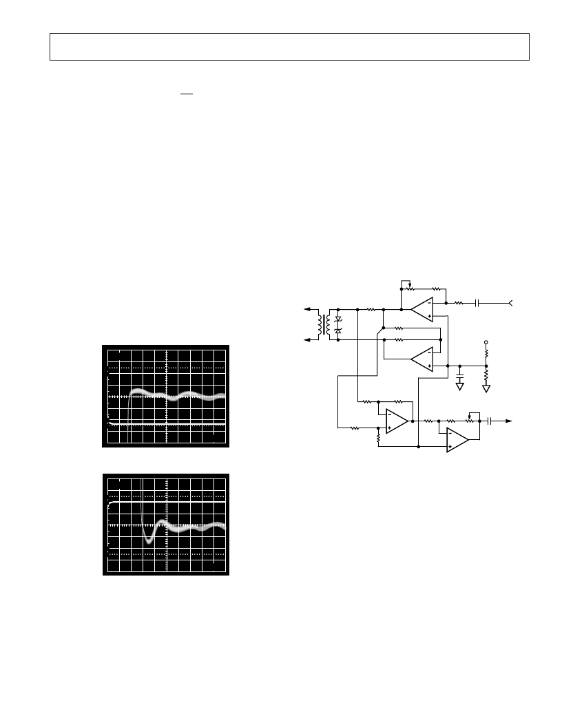
Direct Access Arrangement
Figure 44 shows a schematic for a +5 V single supply transmit/
receive telephone line interface for 600
W
transmission systems.
It allows full duplex transmission of signals on a transformer
coupled 600
W
line. Amplifier A1 provides gain that can be
adjusted to meet the modem output drive requirements. Both
A1 and A2 are configured so as to apply the largest possible
differential signal to the transformer. The largest signal available
on a single +5 V supply is approximately 4.0 V p-p into a 600
W
transmission system. Amplifier A3 is configured as a difference
amplifier to extract the receive information from the transmis-
sion line for amplification by A4. A3 also prevents the transmit
signal from interfering with the receive signal. The gain of A4
can be adjusted in the same manner as A1’s to meet the modem’s
input signal requirements. Standard resistor values permit the
use of SIP (Single In-line Package) format resistor arrays. Couple
this with the OP462 14-lead SOIC or TSSOP package and this
circuit can offer a compact solution.
6.2V
6.2V
TRANSMIT
TXA
RECEIVE
RXA
C1
0.1 F
R1
10k
R2
9.09k
2k
P1
TX GAIN
ADJUST
A1
A2
A3
A4
A1, A2 = 1/2 AD8532
A3, A4 = 1/2 AD8532
Figure 44. A Single-Supply Direct Access Arrangement for
Modems
R3
360
1:1
T1
TO TELEPHONE
LINE
1
2
3
7
6
5
2
3
1
6
5
7
10 F
R7
10k
R8
10k
R5
10k
R6
10k
R9
10k
R14
14.3k
R10
10k
R11
10k
R12
10k
R13
10k
C2
0.1 F
P2
RX GAIN
ADJUST
2k
Z
O
600
5V DC
MIDCOM
671-8005
相關(guān)PDF資料 |
PDF描述 |
|---|---|
| OP162GP | 15 MHz Rail-to-Rail Operational Amplifiers |
| OP162GS | 15 MHz Rail-to-Rail Operational Amplifiers |
| OP262DRU | 15 MHz Rail-to-Rail Operational Amplifiers |
| OP462DRU | 15 MHz Rail-to-Rail Operational Amplifiers |
| OP262GP | 15 MHz Rail-to-Rail Operational Amplifiers |
相關(guān)代理商/技術(shù)參數(shù) |
參數(shù)描述 |
|---|---|
| OP162_05 | 制造商:AD 制造商全稱:Analog Devices 功能描述:15 MHz Rail-to-Rail Operational Amplifiers |
| OP16220100J0G | 制造商:FCI 功能描述:CONNECTOR 制造商:FCI 功能描述:OEM ITEM 505-5BLF-PLUGGABLE SYSTEM |
| OP162DRM-REEL | 制造商:Analog Devices 功能描述:OP AMP SGL GP R-R O/P 6V/12V 8SOIC - Tape and Reel |
| OP162DRMZ-REEL | 制造商:AD 制造商全稱:Analog Devices 功能描述:15 MHz Rail-to-Rail Operational Amplifiers |
| OP162DRU | 制造商:AD 制造商全稱:Analog Devices 功能描述:15 MHz Rail-to-Rail Operational Amplifiers |
發(fā)布緊急采購(gòu),3分鐘左右您將得到回復(fù)。