- 您現(xiàn)在的位置:買賣IC網(wǎng) > PDF目錄378030 > OP462DRU (ANALOG DEVICES INC) 15 MHz Rail-to-Rail Operational Amplifiers PDF資料下載
參數(shù)資料
| 型號: | OP462DRU |
| 廠商: | ANALOG DEVICES INC |
| 元件分類: | 運動控制電子 |
| 英文描述: | 15 MHz Rail-to-Rail Operational Amplifiers |
| 中文描述: | QUAD OP-AMP, 3000 uV OFFSET-MAX, 15 MHz BAND WIDTH, PDSO14 |
| 封裝: | TSSOP-14 |
| 文件頁數(shù): | 11/16頁 |
| 文件大?。?/td> | 1235K |
| 代理商: | OP462DRU |
–11–
REV. D
OP162/OP262/OP462
10
0%
100
90
500ns
2V
50mV
V
S
= 5V
A
V
= 1
R
L
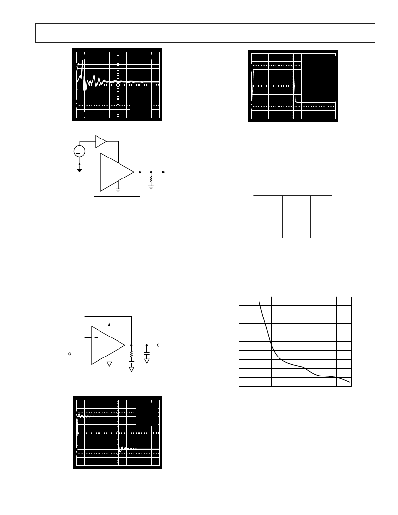
= 10k
Figure 32. Oscilloscope Photo of V
S
and V
OUT
OP462
V
OUT
10k
+1
+
–
0 TO +5V
SQUARE
Figure 33. Test Circuit for Power On Settling Time
Capacitive Load Drive
The OP162/OP262/OP462 is a high speed, extremely accurate
device and can tolerate some capacitive loading at its output.
As load capacitance increases, however, the unity-gain band-
width of the device will decrease. There will also be an increase
in overshoot and settling time for the output. Figure 35 shows
an example of this with the device configured for unity gain and
driving a 10 k
W
resistor and 300 pF capacitor placed in parallel.
By connecting a series R-C network, commonly called a “snub-
ber” network, from the output of the device to ground, this
ringing can be eliminated and overshoot can be significantly
reduced. Figure 34 shows how to set up the snubber network,
and Figure 36 shows the improvement in output response with
the network added.
OPx62
V
IN
V
OUT
+5V
R
X
C
X
C
L
Figure 34. Snubber Network Compensation for Capacitive
Loads
50mV
V
S
= 5V
A
V
= 1
C
L
= 300pF
R
L
= 10k
1 s
100
90
10
0%
Figure 35. A Photo of a Ringing Square Wave
10
0%
100
90
50mV
1 s
V
S
= 5V
A
V
= 1
C
L
= 300pF
R
L
= 10k
WITH SNUBBER:
R
X
= 140
C
X
= 10nF
Figure 36. A Photo of a Nice Square Wave at the Output
The network operates in parallel with the load capacitor, C
L
,
and provides compensation for the added phase lag. The actual
values of the network resistor and capacitor are determined
empirically to minimize overshoot while maximizing unity-gain
bandwidth. Table I shows a few sample snubber networks for
large load capacitors:
Table I. Snubber Networks for Large Capacitive Loads
C
LOAD
R
X
C
X
<300 pF
500 pF
1 nF
10 nF
140
W
100
W
80
W
10
W
10 nF
10 nF
10 nF
47 nF
Obviously, higher load capacitance will also reduce the unity-
gain bandwidth of the device. Figure 37 shows a plot of unity-
gain bandwidth versus capacitive load. The snubber network
will not provide any increase in bandwidth, but it will substan-
tially reduce ringing and overshoot, as shown in the difference
between Figures 35 and 36.
B
C
10
9
0
10pF
10nF
100pF
1nF
4
3
2
1
6
5
8
7
Figure 37. Unity Gain Bandwidth vs. C
LOAD
Total Harmonic Distortion and Crosstalk
The OPx62 device family offers low total harmonic distortion.
This makes it an excellent device choice for audio applications.
Figure 38 shows a graph of THD plus noise figures at 0.001%
for the OP462.
Figure 39 shows a graph of the worst case crosstalk between two
amplifiers in the OP462 device. A 1 V rms signal is applied to
one amplifier while measuring the output of an adjacent ampli-
fier. Both amplifiers are configured for unity gain and supplied
with
±
2.5 V.
相關(guān)PDF資料 |
PDF描述 |
|---|---|
| OP262GP | 15 MHz Rail-to-Rail Operational Amplifiers |
| OP262GS | 15 MHz Rail-to-Rail Operational Amplifiers |
| OP285GP | Dual 9 MHz Precision Operational Amplifier |
| OP285EP | Voltage-Feedback Operational Amplifier |
| OP285ES | Voltage-Feedback Operational Amplifier |
相關(guān)代理商/技術(shù)參數(shù) |
參數(shù)描述 |
|---|---|
| OP462DRU-REEL | 制造商:Analog Devices 功能描述:OP Amp Quad GP R-R O/P ±6V/12V 14-Pin TSSOP T/R 制造商:Rochester Electronics LLC 功能描述: |
| OP462DRUZ-REEL | 制造商:Analog Devices 功能描述: |
| OP462DS | 制造商:Analog Devices 功能描述:OP Amp Quad GP R-R O/P ±6V/12V 14-Pin SOIC N |
| OP462DS-REEL | 制造商:Analog Devices 功能描述:OP Amp Quad GP R-R O/P ±6V/12V 14-Pin SOIC N T/R |
| OP462DS-REEL7 | 制造商:Analog Devices 功能描述:OP Amp Quad GP R-R O/P 制造商:Analog Devices 功能描述:OP Amp Quad GP R-R O/P ±6V/12V 14-Pin SOIC N T/R 制造商:Rochester Electronics LLC 功能描述:LOW COST/POWER 15MHZ RAIL-RAIL OP AMP - Tape and Reel |
發(fā)布緊急采購,3分鐘左右您將得到回復(fù)。