- 您現(xiàn)在的位置:買賣IC網(wǎng) > PDF目錄376245 > OP490E (Analog Devices, Inc.) Low Voltage Micropower Quad Operational Amplifier PDF資料下載
參數(shù)資料
| 型號: | OP490E |
| 廠商: | Analog Devices, Inc. |
| 元件分類: | 運(yùn)動控制電子 |
| 英文描述: | Low Voltage Micropower Quad Operational Amplifier |
| 中文描述: | 低電壓,微功耗四運(yùn)算放大器 |
| 文件頁數(shù): | 9/16頁 |
| 文件大?。?/td> | 206K |
| 代理商: | OP490E |

REV. C
OP490
–9–
1
2
3
4
5
6
7
14
13
12
11
10
9
8
–18V
+18V
GND
C
B
D
A
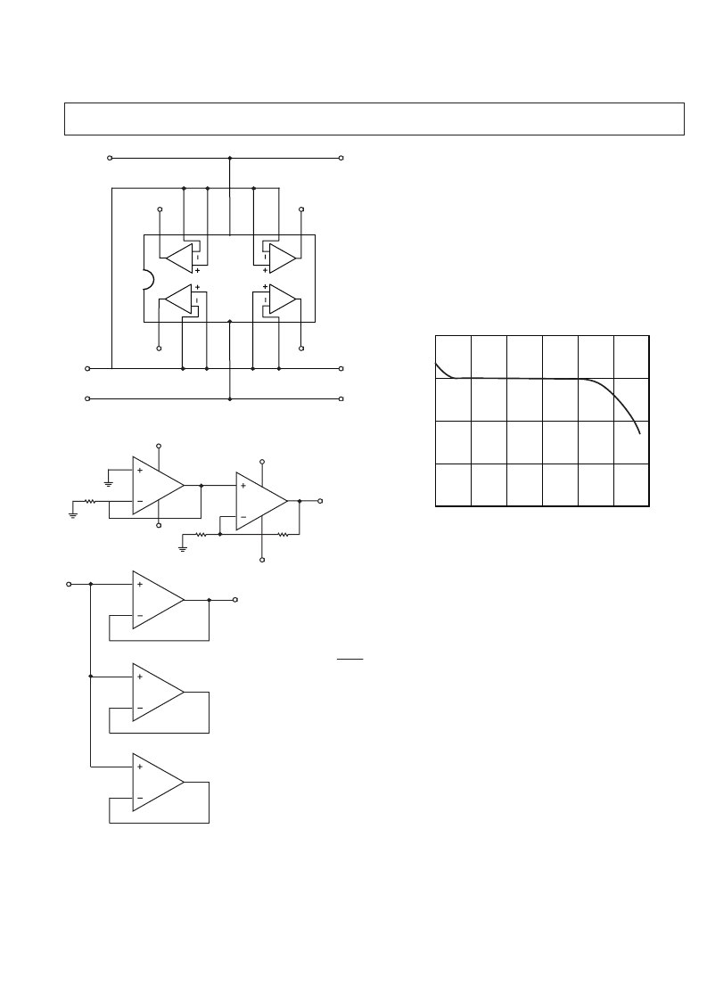
Figure 2. Burn-In Circuit
+15V
–15V
1k
+15V
–15V
V2
100
10k
1/4
OP490A
1/4
OP490B
OP37A
V1
V
IN
1/4
OP490C
1/4
OP490D
20V p-p @ 10Hz
CHANNEL SEPARATION = 20 LOG
V1
V2/1000
Figure 3. Channel Separation Test Circuit
APPLICATIONS INFORMATION
Battery-Powered Applications
The OP490 can be operated on a minimum supply voltage of
1.6 V, or with dual supplies of
±
0.8 V, and draws only 60
m
A of
supply current. In many battery-powered circuits, the OP490
can be continuously operated for hundreds of hours before
requiring battery replacement, reducing equipment downtime,
and operating costs.
High performance portable equipment and instruments fre-
quently use lithium cells because of their long shelf-life, light
weight, and high energy density relative to older primary cells.
Most lithium cells have a nominal output voltage of 3 V and are
noted for a flat discharge characteristic. The low supply current
HOURS
4
3
00
1750
250
L
500
750
2
1
1000
1500
Figure 4. Lithium-Sulphur Dioxide Cell Discharge Charac-
teristic with OP490 and 100 k
W
Loads
requirement of the OP490, combined with the flat discharge
characteristic of the lithium cell, indicates that the OP490 can
be operated over the entire useful life of the cell. Figure 4 shows
the typical discharge characteristic of a 1 Ah lithium cell power-
ing an OP490 with each amplifier, in turn, driving full output
swing into a 100 k
W
load.
Single-Supply Output Voltage Range
In single-supply operation the OP490’s input and output ranges
include ground. This allows true “zero-in, zero-out” operation.
The output stage provides an active pull-down to around 0.8 V
above ground. Below this level, a load resistance of up to 1 M
W
to ground is required to pull the output down to zero.
In the region from ground to 0.8 V, the OP490 has voltage gain
equal to the data sheet specification. Output current source
capability is maintained over the entire voltage range including
ground.
Input Voltage Protection
The OP490 uses a PNP input stage with protection resistors in
series with the inverting and noninverting inputs. The high
breakdown of the PNP transistors coupled with the protection
resistors provides a large amount of input protection, allowing
the inputs to be taken 20 V beyond either supply without dam-
aging the amplifier.
相關(guān)PDF資料 |
PDF描述 |
|---|---|
| OP490F | Low Voltage Micropower Quad Operational Amplifier |
| op490 | Low Voltage Micropower Quad Operational Amplifier(低電壓微功率四運(yùn)放) |
| op492 | Quad OP AMP(四運(yùn)算放大器) |
| op292 | Dual OP AMP(雙運(yùn)算放大器) |
| OP492 | DUAL/QUAD SINGLE SUPPLY OPERATIONAL AMPLIFIER |
相關(guān)代理商/技術(shù)參數(shù) |
參數(shù)描述 |
|---|---|
| OP490EY | 制造商:Rochester Electronics LLC 功能描述:MICROPOWER QUAD OP AMP IC - Bulk 制造商:Analog Devices 功能描述: |
| OP490F | 制造商:AD 制造商全稱:Analog Devices 功能描述:Low Voltage Micropower Quad Operational Amplifier |
| OP490FY | 制造商:Rochester Electronics LLC 功能描述:MICROPOWER QUAD OP AMP IC - Bulk 制造商:Analog Devices 功能描述: |
| OP490G | 制造商:AD 制造商全稱:Analog Devices 功能描述:Low Voltage Micropower Quad Operational Amplifier |
| OP490GBC | 制造商:Analog Devices 功能描述: |
發(fā)布緊急采購,3分鐘左右您將得到回復(fù)。