- 您現(xiàn)在的位置:買賣IC網(wǎng) > PDF目錄224633 > OR2C10A-6S208I (Electronic Theatre Controls, Inc.) Field-Programmable Gate Arrays PDF資料下載
參數(shù)資料
| 型號: | OR2C10A-6S208I |
| 廠商: | Electronic Theatre Controls, Inc. |
| 元件分類: | FPGA |
| 英文描述: | Field-Programmable Gate Arrays |
| 中文描述: | 現(xiàn)場可編程門陣列 |
| 文件頁數(shù): | 41/192頁 |
| 文件大?。?/td> | 3148K |
| 代理商: | OR2C10A-6S208I |
Data Sheet
June 1999
ORCA Series 2 FPGAs
Lucent Technologies Inc.
135
Timing Characteristics (continued)
1.The input buffers contain a programmable delay to allow the hold time vs. the external clock pin to be equal to 0.
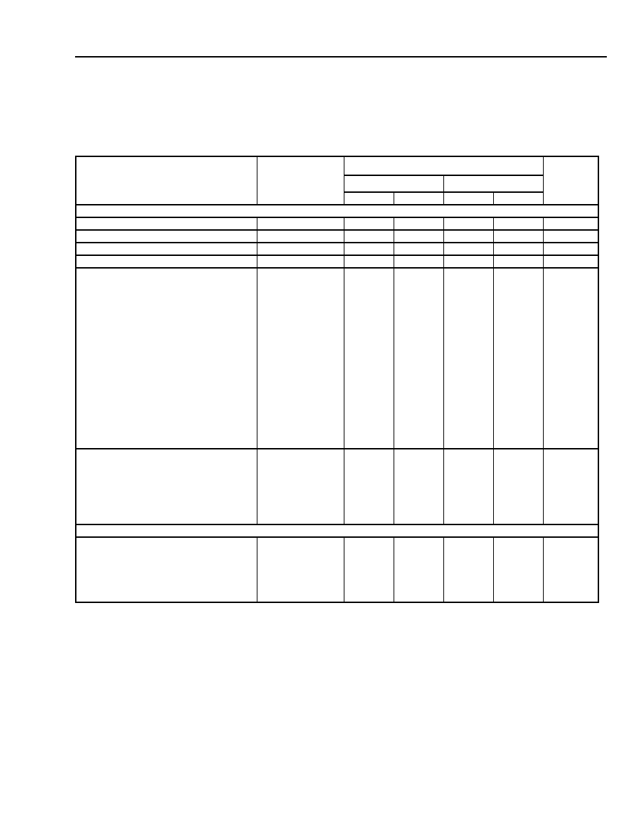
Table 33B. OR2TxxB Sequential PFU Timing Characteristics
OR2TxxB Commercial: VDD = 3.0 V to 3.6 V, 0 °C
≤ TA ≤ 70 °C; OR2TxxB Industrial: VDD = 3.0 V to 3.6 V, –40 °C ≤ TA ≤
+85 °C.
Parameter
Symbol
Speed
Unit
-7
-8
Min
Max
Min
Max
Input Requirements
Clock Low Time
TCL
1.7
—
1.4
—
ns
Clock High Time
TCH
1.7
—
1.4
—
ns
Global S/R Pulse Width (GSRN)
TRW
1.7
—
1.4
—
ns
Local S/R Pulse Width
TPW
1.7
—
1.4
—
ns
Combinatorial Setup Times (TJ = 85 °C,
VDD = min):
Four Input Variables to Clock
(A[4:0], B[4:0] to CK)
Five Input Variables to Clock
(A[4:0], B[4:0] to CK)
PFUMUX to Clock (A[4:0], B[4:0] to CK)
PFUMUX to Clock (C0 to CK)
PFUNAND to Clock (A[4:0], B[4:0] to CK)
PFUNAND to Clock (C0 to CK)
PFUXOR to Clock (A[4:0], B[4:0] to CK)
PFUXOR to Clock (C0 to CK)
Data In to Clock (WD[3:0] to CK)
Clock Enable to Clock (CE to CK)
Local Set/Reset (synchronous) (LSR to CK)
Data Select to Clock (SEL to CK)
Pad Direct In
F4*_SET
F5*_SET
MUX_SET
C0MUX_SET
ND_SET
C0ND_SET
XOR_SET
C0XOR_SET
D*_SET
CKEN_SET
LSR_SET
SELECT_SET
PDIN_SET
1.0
1.3
1.1
1.0
0.8
1.3
1.1
0.2
1.0
0.0
—
0.8
1.3
0.8
0.7
1.3
0.8
0.1
0.8
0.0
—
ns
Combinatorial Hold Times (TJ = all, VDD = all):
Data In (WD[3:0] from CK)
Clock Enable (CE from CK)
Local Set/Reset (synchronous) (LSR from CK)
Data Select (SEL from CK)
Pad Direct In Hold (DIA[3:0], DIB[3:0] to CK)1
All Others
D*_HLD
CKEN_HLD
LSR_HLD
SELECT_HLD
PDIN_HLD
—
0.0
0.1
0.0
—
0.0
0.1
0.0
—
ns
Output Characteristics
Sequential Delays (TJ = 85 °C, VDD = min):
Local S/R (async) to PFU Out (LSR to Q[3:0])
Global S/R to PFU Out (GSRN to Q[3:0])
Clock to PFU Out (CK to Q[3:0])—Register
Clock to PFU Out (CK to Q[3:0])—Latch
Transparent Latch (WD[3:0] to Q[3:0])
LSR_DEL
GSR_DEL
REG_DEL
LTCH_DEL
LTCH_DDEL
2.2
1.4
1.0
1.7
—
1.8
1.0
1.4
—
ns
相關(guān)PDF資料 |
PDF描述 |
|---|---|
| OR2C10A-6S240 | Field-Programmable Gate Arrays |
| OR2C10A-6S240I | Field-Programmable Gate Arrays |
| OR2C10A-6S256 | Ceramic Chip Capacitors / MIL-PRF-55681; Capacitance [nom]: 18pF; Working Voltage (Vdc)[max]: 100V; Capacitance Tolerance: +/-10%; Dielectric: Multilayer Ceramic; Temperature Coefficient: C0G (NP0); Lead Style: Surface Mount Chip; Lead Dimensions: 0805; Termination: Solder Coated SnPb; Body Dimensions: 0.080" x 0.050" x 0.055"; Container: Bag; Features: MIL-PRF-55681: M Failure Rate |
| OR2C10A-6S256I | Field-Programmable Gate Arrays |
| OR2C10A-6S352 | Field-Programmable Gate Arrays |
相關(guān)代理商/技術(shù)參數(shù) |
參數(shù)描述 |
|---|---|
| OR2C12A3BA256I-DB | 功能描述:FPGA - 現(xiàn)場可編程門陣列 1296 LUT 288 I/O RoHS:否 制造商:Altera Corporation 系列:Cyclone V E 柵極數(shù)量: 邏輯塊數(shù)量:943 內(nèi)嵌式塊RAM - EBR:1956 kbit 輸入/輸出端數(shù)量:128 最大工作頻率:800 MHz 工作電源電壓:1.1 V 最大工作溫度:+ 70 C 安裝風(fēng)格:SMD/SMT 封裝 / 箱體:FBGA-256 |
| OR2C12A3BA352I-DB | 功能描述:FPGA - 現(xiàn)場可編程門陣列 Use ECP/EC or XP RoHS:否 制造商:Altera Corporation 系列:Cyclone V E 柵極數(shù)量: 邏輯塊數(shù)量:943 內(nèi)嵌式塊RAM - EBR:1956 kbit 輸入/輸出端數(shù)量:128 最大工作頻率:800 MHz 工作電源電壓:1.1 V 最大工作溫度:+ 70 C 安裝風(fēng)格:SMD/SMT 封裝 / 箱體:FBGA-256 |
| OR2C12A3M84I-D | 功能描述:FPGA - 現(xiàn)場可編程門陣列 1296 LUT 288 I/O RoHS:否 制造商:Altera Corporation 系列:Cyclone V E 柵極數(shù)量: 邏輯塊數(shù)量:943 內(nèi)嵌式塊RAM - EBR:1956 kbit 輸入/輸出端數(shù)量:128 最大工作頻率:800 MHz 工作電源電壓:1.1 V 最大工作溫度:+ 70 C 安裝風(fēng)格:SMD/SMT 封裝 / 箱體:FBGA-256 |
| OR2C12A3S208-DB | 功能描述:FPGA - 現(xiàn)場可編程門陣列 1296 LUT 288 I/O RoHS:否 制造商:Altera Corporation 系列:Cyclone V E 柵極數(shù)量: 邏輯塊數(shù)量:943 內(nèi)嵌式塊RAM - EBR:1956 kbit 輸入/輸出端數(shù)量:128 最大工作頻率:800 MHz 工作電源電壓:1.1 V 最大工作溫度:+ 70 C 安裝風(fēng)格:SMD/SMT 封裝 / 箱體:FBGA-256 |
| OR2C12A3S208-DBA1357 | 制造商:Rochester Electronics LLC 功能描述:- Bulk |
發(fā)布緊急采購,3分鐘左右您將得到回復(fù)。