- 您現(xiàn)在的位置:買(mǎi)賣(mài)IC網(wǎng) > PDF目錄224634 > OR2C10A-7PS352 (Electronic Theatre Controls, Inc.) Field-Programmable Gate Arrays PDF資料下載
參數(shù)資料
| 型號(hào): | OR2C10A-7PS352 |
| 廠商: | Electronic Theatre Controls, Inc. |
| 元件分類(lèi): | FPGA |
| 英文描述: | Field-Programmable Gate Arrays |
| 中文描述: | 現(xiàn)場(chǎng)可編程門(mén)陣列 |
| 文件頁(yè)數(shù): | 118/192頁(yè) |
| 文件大?。?/td> | 3148K |
| 代理商: | OR2C10A-7PS352 |
第1頁(yè)第2頁(yè)第3頁(yè)第4頁(yè)第5頁(yè)第6頁(yè)第7頁(yè)第8頁(yè)第9頁(yè)第10頁(yè)第11頁(yè)第12頁(yè)第13頁(yè)第14頁(yè)第15頁(yè)第16頁(yè)第17頁(yè)第18頁(yè)第19頁(yè)第20頁(yè)第21頁(yè)第22頁(yè)第23頁(yè)第24頁(yè)第25頁(yè)第26頁(yè)第27頁(yè)第28頁(yè)第29頁(yè)第30頁(yè)第31頁(yè)第32頁(yè)第33頁(yè)第34頁(yè)第35頁(yè)第36頁(yè)第37頁(yè)第38頁(yè)第39頁(yè)第40頁(yè)第41頁(yè)第42頁(yè)第43頁(yè)第44頁(yè)第45頁(yè)第46頁(yè)第47頁(yè)第48頁(yè)第49頁(yè)第50頁(yè)第51頁(yè)第52頁(yè)第53頁(yè)第54頁(yè)第55頁(yè)第56頁(yè)第57頁(yè)第58頁(yè)第59頁(yè)第60頁(yè)第61頁(yè)第62頁(yè)第63頁(yè)第64頁(yè)第65頁(yè)第66頁(yè)第67頁(yè)第68頁(yè)第69頁(yè)第70頁(yè)第71頁(yè)第72頁(yè)第73頁(yè)第74頁(yè)第75頁(yè)第76頁(yè)第77頁(yè)第78頁(yè)第79頁(yè)第80頁(yè)第81頁(yè)第82頁(yè)第83頁(yè)第84頁(yè)第85頁(yè)第86頁(yè)第87頁(yè)第88頁(yè)第89頁(yè)第90頁(yè)第91頁(yè)第92頁(yè)第93頁(yè)第94頁(yè)第95頁(yè)第96頁(yè)第97頁(yè)第98頁(yè)第99頁(yè)第100頁(yè)第101頁(yè)第102頁(yè)第103頁(yè)第104頁(yè)第105頁(yè)第106頁(yè)第107頁(yè)第108頁(yè)第109頁(yè)第110頁(yè)第111頁(yè)第112頁(yè)第113頁(yè)第114頁(yè)第115頁(yè)第116頁(yè)第117頁(yè)當(dāng)前第118頁(yè)第119頁(yè)第120頁(yè)第121頁(yè)第122頁(yè)第123頁(yè)第124頁(yè)第125頁(yè)第126頁(yè)第127頁(yè)第128頁(yè)第129頁(yè)第130頁(yè)第131頁(yè)第132頁(yè)第133頁(yè)第134頁(yè)第135頁(yè)第136頁(yè)第137頁(yè)第138頁(yè)第139頁(yè)第140頁(yè)第141頁(yè)第142頁(yè)第143頁(yè)第144頁(yè)第145頁(yè)第146頁(yè)第147頁(yè)第148頁(yè)第149頁(yè)第150頁(yè)第151頁(yè)第152頁(yè)第153頁(yè)第154頁(yè)第155頁(yè)第156頁(yè)第157頁(yè)第158頁(yè)第159頁(yè)第160頁(yè)第161頁(yè)第162頁(yè)第163頁(yè)第164頁(yè)第165頁(yè)第166頁(yè)第167頁(yè)第168頁(yè)第169頁(yè)第170頁(yè)第171頁(yè)第172頁(yè)第173頁(yè)第174頁(yè)第175頁(yè)第176頁(yè)第177頁(yè)第178頁(yè)第179頁(yè)第180頁(yè)第181頁(yè)第182頁(yè)第183頁(yè)第184頁(yè)第185頁(yè)第186頁(yè)第187頁(yè)第188頁(yè)第189頁(yè)第190頁(yè)第191頁(yè)第192頁(yè)
Data Sheet
June 1999
ORCA Series 2 FPGAs
Lucent Technologies Inc.
31
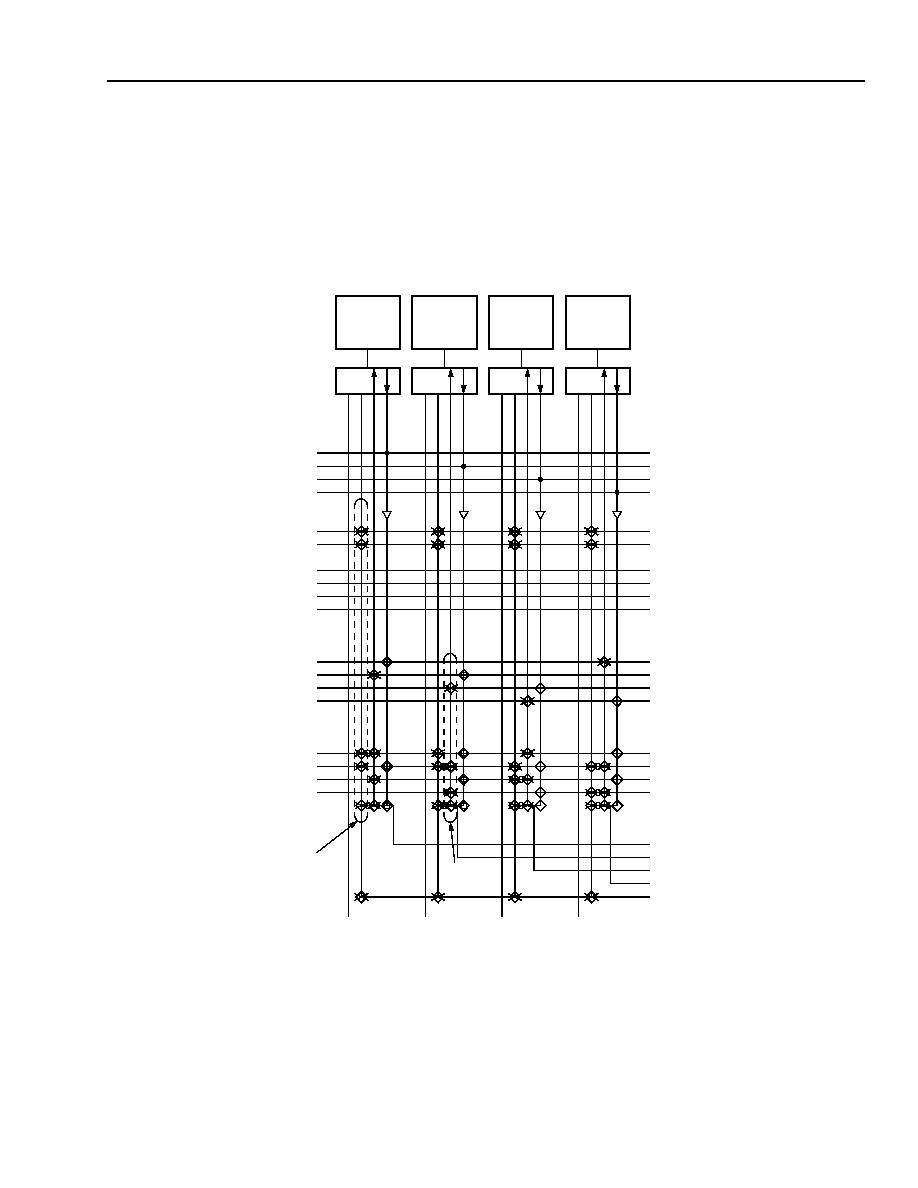
Programmable Input/Output Cells
(continued)
Figure 27 shows paths to and from pads and the use of MUX CIPs to connect lines. Detail A shows six MUX CIPs
for the pad P0 used to construct the net for the 3-state signal. In the MUX CIP, one of six lines is connected to a line
to form the net. In this case, the ts0 signal can be driven by either of the two PXLs, PX1[0], PX1[1], XSW[0], or the
LLDRV lines. Detail B shows the four MUX CIPs used to drive the P1 output. The source line for OUT1 is either
XSW[1], PX1[1], PX1[3], or PX2[2].
5-2843.BL(F).2C.r3
Figure 27. PIC Detail
DT
PA
PB
PC
PD
TS
0
OUT0
IN0
DOUT0
TS
1
OUT1
IN1
DOUT1
TS
3
OUT3
IN3
DOUT3
TS
2
OUT2
IN2
DOUT2
PXL[1]
PXL[0]
PX2[2]
PX2[3]
PX2[0]
PX2[1]
PX1[0]
PX1[1]
PX1[2]
PX1[3]
PXH[1]
PXH[2]
PXH[3]
PXH[0]
PXL[1]
PXL[0]
PX2[2]
PX2[3]
PX2[0]
PX2[1]
PX1[0]
PX1[1]
PX1[2]
PX1[3]
PXH[1]
PXH[2]
PXH[3]
PXH[0]
DOUT[0]
DOUT[1]
DOUT[2]
DOUT[3]
XSW[0]
XSW[1]
XSW[2]
XSW[3]
LLDRV
A
B
相關(guān)PDF資料 |
PDF描述 |
|---|---|
| OR2C10A-7PS352I | Field-Programmable Gate Arrays |
| OR2C10A-7PS84 | Field-Programmable Gate Arrays |
| OR2C10A-7PS84I | Field-Programmable Gate Arrays |
| OR2C10A-7S160 | Ceramic Chip Capacitors / MIL-PRF-55681; Capacitance [nom]: 1.2pF; Working Voltage (Vdc)[max]: 100V; Capacitance Tolerance: +/-0.25pF; Dielectric: Multilayer Ceramic; Temperature Coefficient: C0G (NP0); Lead Style: Surface Mount Chip; Lead Dimensions: 0805; Termination: Solder Coated SnPb; Body Dimensions: 0.080" x 0.050" x 0.055"; Container: Bag; Features: MIL-PRF-55681: R Failure Rate |
| OR2C10A-7S160I | Field-Programmable Gate Arrays |
相關(guān)代理商/技術(shù)參數(shù) |
參數(shù)描述 |
|---|---|
| OR2C12A3BA256I-DB | 功能描述:FPGA - 現(xiàn)場(chǎng)可編程門(mén)陣列 1296 LUT 288 I/O RoHS:否 制造商:Altera Corporation 系列:Cyclone V E 柵極數(shù)量: 邏輯塊數(shù)量:943 內(nèi)嵌式塊RAM - EBR:1956 kbit 輸入/輸出端數(shù)量:128 最大工作頻率:800 MHz 工作電源電壓:1.1 V 最大工作溫度:+ 70 C 安裝風(fēng)格:SMD/SMT 封裝 / 箱體:FBGA-256 |
| OR2C12A3BA352I-DB | 功能描述:FPGA - 現(xiàn)場(chǎng)可編程門(mén)陣列 Use ECP/EC or XP RoHS:否 制造商:Altera Corporation 系列:Cyclone V E 柵極數(shù)量: 邏輯塊數(shù)量:943 內(nèi)嵌式塊RAM - EBR:1956 kbit 輸入/輸出端數(shù)量:128 最大工作頻率:800 MHz 工作電源電壓:1.1 V 最大工作溫度:+ 70 C 安裝風(fēng)格:SMD/SMT 封裝 / 箱體:FBGA-256 |
| OR2C12A3M84I-D | 功能描述:FPGA - 現(xiàn)場(chǎng)可編程門(mén)陣列 1296 LUT 288 I/O RoHS:否 制造商:Altera Corporation 系列:Cyclone V E 柵極數(shù)量: 邏輯塊數(shù)量:943 內(nèi)嵌式塊RAM - EBR:1956 kbit 輸入/輸出端數(shù)量:128 最大工作頻率:800 MHz 工作電源電壓:1.1 V 最大工作溫度:+ 70 C 安裝風(fēng)格:SMD/SMT 封裝 / 箱體:FBGA-256 |
| OR2C12A3S208-DB | 功能描述:FPGA - 現(xiàn)場(chǎng)可編程門(mén)陣列 1296 LUT 288 I/O RoHS:否 制造商:Altera Corporation 系列:Cyclone V E 柵極數(shù)量: 邏輯塊數(shù)量:943 內(nèi)嵌式塊RAM - EBR:1956 kbit 輸入/輸出端數(shù)量:128 最大工作頻率:800 MHz 工作電源電壓:1.1 V 最大工作溫度:+ 70 C 安裝風(fēng)格:SMD/SMT 封裝 / 箱體:FBGA-256 |
| OR2C12A3S208-DBA1357 | 制造商:Rochester Electronics LLC 功能描述:- Bulk |
發(fā)布緊急采購(gòu),3分鐘左右您將得到回復(fù)。