- 您現(xiàn)在的位置:買賣IC網(wǎng) > PDF目錄224637 > OR2C12A-6BA256 (Electronic Theatre Controls, Inc.) Field-Programmable Gate Arrays PDF資料下載
參數(shù)資料
| 型號: | OR2C12A-6BA256 |
| 廠商: | Electronic Theatre Controls, Inc. |
| 元件分類: | FPGA |
| 英文描述: | Field-Programmable Gate Arrays |
| 中文描述: | 現(xiàn)場可編程門陣列 |
| 文件頁數(shù): | 117/192頁 |
| 文件大小: | 3148K |
| 代理商: | OR2C12A-6BA256 |
第1頁第2頁第3頁第4頁第5頁第6頁第7頁第8頁第9頁第10頁第11頁第12頁第13頁第14頁第15頁第16頁第17頁第18頁第19頁第20頁第21頁第22頁第23頁第24頁第25頁第26頁第27頁第28頁第29頁第30頁第31頁第32頁第33頁第34頁第35頁第36頁第37頁第38頁第39頁第40頁第41頁第42頁第43頁第44頁第45頁第46頁第47頁第48頁第49頁第50頁第51頁第52頁第53頁第54頁第55頁第56頁第57頁第58頁第59頁第60頁第61頁第62頁第63頁第64頁第65頁第66頁第67頁第68頁第69頁第70頁第71頁第72頁第73頁第74頁第75頁第76頁第77頁第78頁第79頁第80頁第81頁第82頁第83頁第84頁第85頁第86頁第87頁第88頁第89頁第90頁第91頁第92頁第93頁第94頁第95頁第96頁第97頁第98頁第99頁第100頁第101頁第102頁第103頁第104頁第105頁第106頁第107頁第108頁第109頁第110頁第111頁第112頁第113頁第114頁第115頁第116頁當(dāng)前第117頁第118頁第119頁第120頁第121頁第122頁第123頁第124頁第125頁第126頁第127頁第128頁第129頁第130頁第131頁第132頁第133頁第134頁第135頁第136頁第137頁第138頁第139頁第140頁第141頁第142頁第143頁第144頁第145頁第146頁第147頁第148頁第149頁第150頁第151頁第152頁第153頁第154頁第155頁第156頁第157頁第158頁第159頁第160頁第161頁第162頁第163頁第164頁第165頁第166頁第167頁第168頁第169頁第170頁第171頁第172頁第173頁第174頁第175頁第176頁第177頁第178頁第179頁第180頁第181頁第182頁第183頁第184頁第185頁第186頁第187頁第188頁第189頁第190頁第191頁第192頁
Data Sheet
ORCA Series 2 FPGAs
June 1999
30
Lucent Technologies Inc.
Programmable Input/Output Cells (continued)
5-2843(F).r8
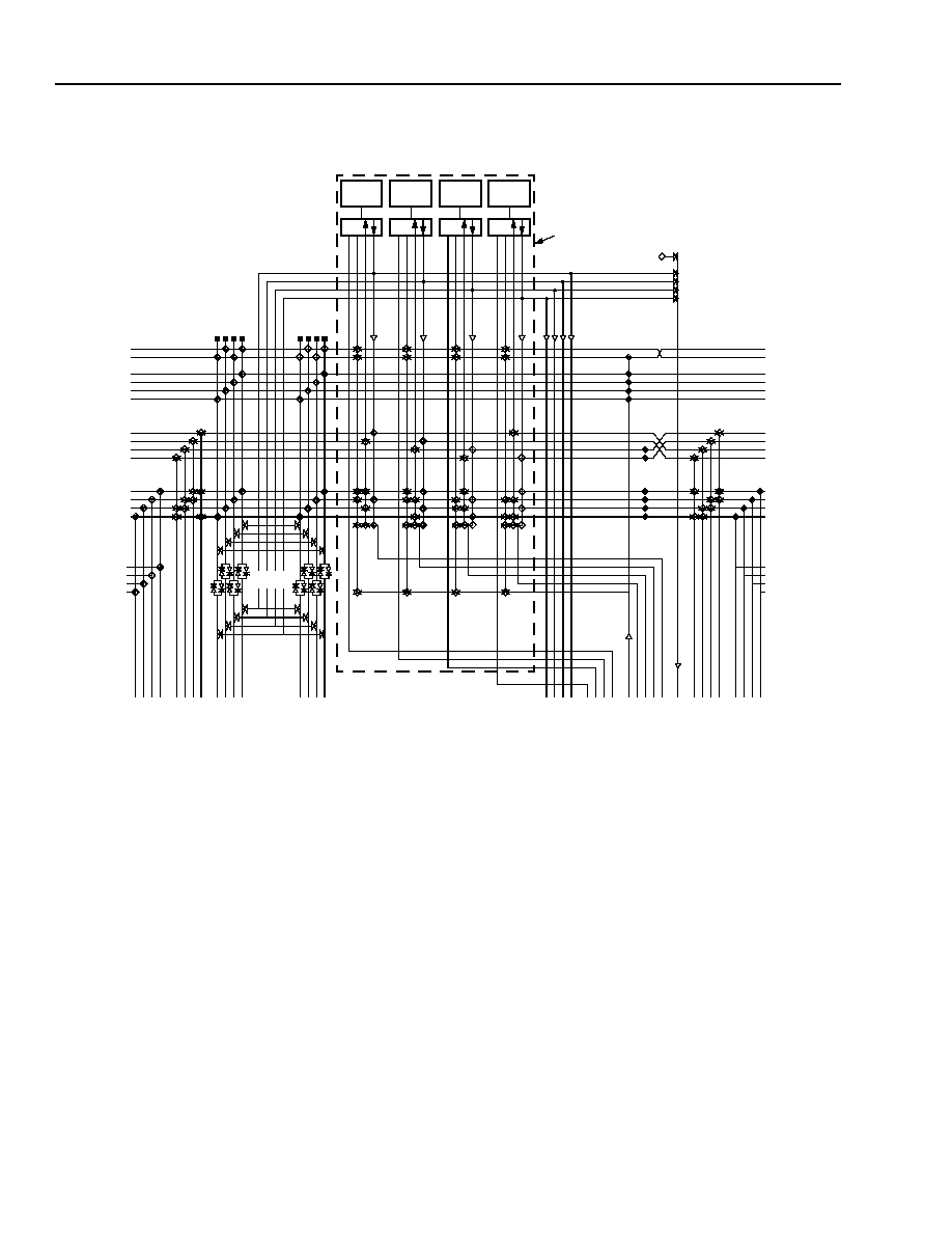
Figure 26. PIC Architecture
DT
PA
PB
PC
PD
PXL[1]
PXL[0]
PX2[2]
PX2[3]
PX2[0]
PX2[1]
PX1[0]
PX1[1]
PX1[2]
PX1[3]
PXH[1]
PXH[2]
PXH[3]
PXH[0]
B
A
C
D
FE
G
Q
PXL[0]
PXL[1]
PX2[0]
PX2[1]
PX2[2]
PX2[3]
PX1[0]
PX1[1]
PX1[2]
PX1[3]
PXH[1]
PXH[2]
PXH[3]
PXH[0]
B
A
C
D
TS
0
OU
T0
IN
0
DO
UT
0
TS
1
OU
T1
IN
1
DO
UT
1
TS
3
OU
T3
IN
3
DO
UT
3
TS
2
OU
T2
IN
2
DO
UT
2
PIC DETAIL
BI
D
I3
F
O
N
O
LLDRV
M
I
L
J
K
N
D
C
P
Q
M
B
IDIH3
B
IDIH2
B
IDIH1
B
IDIH0
BI
D
I2
BI
D
I1
BI
D
I0
LL
IN
3
LL
IN
2
LL
IN
1
LL
IN
0
P
VX
L
[3
]
VX
L
[2
]
VX
L
[1
]
VX
L
[0
]
VX
1
[7
]
VX
1
[6
]
VX
1
[5
]
VX
1
[4
]
VX
1
[3
]
VX
1
[2
]
VX
1
[1
]
VX
1
[0
]
DO
UT
[3
]
DO
UT
[2
]
DO
UT
[1
]
XS
W
[3
]
XS
W
[2
]
XS
W
[1
]
XS
W
[0
]
XS
W
[4
]
DO
UT
[0
]
CK
T
VXH
[3
]
VXH
[2
]
VXH
[1
]
VXH
[0
]
VX
4
[7
]
VX
4
[6
]
VX
4
[5
]
VX
4
[4
]
P
D
IN
T
B
[3
]
P
D
IN
T
B
[2
]
P
D
IN
T
B
[1
]
P
D
IN
T
B
[0
]
VX
4
[3
]
VX
4
[2
]
VX
4
[1
]
VX
4
[0
]
PLC-PIC Routing Resources
There is no direct connection between the inter-PIC
lines and the PLC lines. All connections to/from the
PLC must be done through the connecting lines which
are perpendicular to the lines in the PIC. The use of
perpendicular and parallel lines will be clearer if the
PLC and PIC architectures (Figure 23 and Figure 26)
are placed side by side. Twenty-nine lines in the PLC
can be connected to the 15 lines in the PIC.
Multiple connections between the PIC PX1 lines and
the PLC X1 lines are available. These allow buses
placed in any arbitrary order on the I/O pads to be
unscrambled when placed on the PLC X1 lines. Con-
nections are also available between the PIC PX2 lines
and the PLC X1 lines.
There are eight tridirectional (four TRIDI/four TRIDIH)
buffers in each PIC; they can do the following:
s
Drive a signal from an I/O pad onto one of the adja-
cent PLC’s XL or XH lines
s
Drive a signal from an I/O pad onto one of the two
PXL or four PXH lines in the PIC
s
Drive a signal from the PLC XL or XH lines onto one
of the two PXL or four PXH lines in the PIC
s
Drive a signal from the PIC PXL or PXH lines onto
one of the PLC XL or XH lines
相關(guān)PDF資料 |
PDF描述 |
|---|---|
| OR2C12A-6BA256I | Field-Programmable Gate Arrays |
| OR2C12A-6BA304 | Field-Programmable Gate Arrays |
| OR2C12A-6BA304I | Field-Programmable Gate Arrays |
| OR2C12A-6BA352 | Field-Programmable Gate Arrays |
| OR2C12A-6BA352I | Field-Programmable Gate Arrays |
相關(guān)代理商/技術(shù)參數(shù) |
參數(shù)描述 |
|---|---|
| OR2C15A3BA256I-DB | 功能描述:FPGA - 現(xiàn)場可編程門陣列 1600 LUT 298 I/O RoHS:否 制造商:Altera Corporation 系列:Cyclone V E 柵極數(shù)量: 邏輯塊數(shù)量:943 內(nèi)嵌式塊RAM - EBR:1956 kbit 輸入/輸出端數(shù)量:128 最大工作頻率:800 MHz 工作電源電壓:1.1 V 最大工作溫度:+ 70 C 安裝風(fēng)格:SMD/SMT 封裝 / 箱體:FBGA-256 |
| OR2C15A3BA352I-DB | 功能描述:FPGA - 現(xiàn)場可編程門陣列 Use ECP/EC or XP RoHS:否 制造商:Altera Corporation 系列:Cyclone V E 柵極數(shù)量: 邏輯塊數(shù)量:943 內(nèi)嵌式塊RAM - EBR:1956 kbit 輸入/輸出端數(shù)量:128 最大工作頻率:800 MHz 工作電源電壓:1.1 V 最大工作溫度:+ 70 C 安裝風(fēng)格:SMD/SMT 封裝 / 箱體:FBGA-256 |
| OR2C15A3M84I-D | 功能描述:FPGA - 現(xiàn)場可編程門陣列 1600 LUT 298 I/O RoHS:否 制造商:Altera Corporation 系列:Cyclone V E 柵極數(shù)量: 邏輯塊數(shù)量:943 內(nèi)嵌式塊RAM - EBR:1956 kbit 輸入/輸出端數(shù)量:128 最大工作頻率:800 MHz 工作電源電壓:1.1 V 最大工作溫度:+ 70 C 安裝風(fēng)格:SMD/SMT 封裝 / 箱體:FBGA-256 |
| OR2C15A3PS208I-DB | 功能描述:FPGA - 現(xiàn)場可編程門陣列 1600 LUT 298 I/O RoHS:否 制造商:Altera Corporation 系列:Cyclone V E 柵極數(shù)量: 邏輯塊數(shù)量:943 內(nèi)嵌式塊RAM - EBR:1956 kbit 輸入/輸出端數(shù)量:128 最大工作頻率:800 MHz 工作電源電壓:1.1 V 最大工作溫度:+ 70 C 安裝風(fēng)格:SMD/SMT 封裝 / 箱體:FBGA-256 |
| OR2C15A3PS240I-DB | 功能描述:FPGA - 現(xiàn)場可編程門陣列 1600 LUT 298 I/O RoHS:否 制造商:Altera Corporation 系列:Cyclone V E 柵極數(shù)量: 邏輯塊數(shù)量:943 內(nèi)嵌式塊RAM - EBR:1956 kbit 輸入/輸出端數(shù)量:128 最大工作頻率:800 MHz 工作電源電壓:1.1 V 最大工作溫度:+ 70 C 安裝風(fēng)格:SMD/SMT 封裝 / 箱體:FBGA-256 |
發(fā)布緊急采購,3分鐘左右您將得到回復(fù)。