- 您現(xiàn)在的位置:買賣IC網(wǎng) > PDF目錄299575 > OR3T306S240I-DB (LATTICE SEMICONDUCTOR CORP) FPGA, 196 CLBS, 48000 GATES, PQFP240 PDF資料下載
參數(shù)資料
| 型號(hào): | OR3T306S240I-DB |
| 廠商: | LATTICE SEMICONDUCTOR CORP |
| 元件分類: | FPGA |
| 英文描述: | FPGA, 196 CLBS, 48000 GATES, PQFP240 |
| 封裝: | PLASTIC, SQFP-240 |
| 文件頁數(shù): | 138/203頁 |
| 文件大小: | 1368K |
| 代理商: | OR3T306S240I-DB |
第1頁第2頁第3頁第4頁第5頁第6頁第7頁第8頁第9頁第10頁第11頁第12頁第13頁第14頁第15頁第16頁第17頁第18頁第19頁第20頁第21頁第22頁第23頁第24頁第25頁第26頁第27頁第28頁第29頁第30頁第31頁第32頁第33頁第34頁第35頁第36頁第37頁第38頁第39頁第40頁第41頁第42頁第43頁第44頁第45頁第46頁第47頁第48頁第49頁第50頁第51頁第52頁第53頁第54頁第55頁第56頁第57頁第58頁第59頁第60頁第61頁第62頁第63頁第64頁第65頁第66頁第67頁第68頁第69頁第70頁第71頁第72頁第73頁第74頁第75頁第76頁第77頁第78頁第79頁第80頁第81頁第82頁第83頁第84頁第85頁第86頁第87頁第88頁第89頁第90頁第91頁第92頁第93頁第94頁第95頁第96頁第97頁第98頁第99頁第100頁第101頁第102頁第103頁第104頁第105頁第106頁第107頁第108頁第109頁第110頁第111頁第112頁第113頁第114頁第115頁第116頁第117頁第118頁第119頁第120頁第121頁第122頁第123頁第124頁第125頁第126頁第127頁第128頁第129頁第130頁第131頁第132頁第133頁第134頁第135頁第136頁第137頁當(dāng)前第138頁第139頁第140頁第141頁第142頁第143頁第144頁第145頁第146頁第147頁第148頁第149頁第150頁第151頁第152頁第153頁第154頁第155頁第156頁第157頁第158頁第159頁第160頁第161頁第162頁第163頁第164頁第165頁第166頁第167頁第168頁第169頁第170頁第171頁第172頁第173頁第174頁第175頁第176頁第177頁第178頁第179頁第180頁第181頁第182頁第183頁第184頁第185頁第186頁第187頁第188頁第189頁第190頁第191頁第192頁第193頁第194頁第195頁第196頁第197頁第198頁第199頁第200頁第201頁第202頁第203頁
4
Lattice Semiconductor
Data Sheet
November 2006
ORCA Series 3C and 3T FPGAs
System-Level Features
System-level features reduce glue logic requirements
and make a system on a chip possible. These features
in the
ORCA Series 3 include:
■ Full PCI local bus compliance.
■ Dual-use microprocessor interface (MPI) can be
used for conguration, readback, device control, and
device status, as well as for a general-purpose inter-
face to the FPGA. Glueless interface to
i960* and
PowerPC processors with user-congurable
address space provided.
■ Parallel readback of conguration data capability with
the built-in microprocessor interface.
■ Programmable clock manager (PCM) adjusts clock
phase and duty cycle for input clock rates from
5 MHz to 120 MHz. The PCM may be combined with
FPGA logic to create complex functions, such as dig-
ital phase-locked loops (DPLL), frequency counters,
and frequency synthesizers or clock doublers. Two
PCMs are provided per device.
■ True, internal, 3-state, bidirectional buses with simple
control provided by the SLIC.
■ 32 x 4 RAM per PFU, congurable as single- or dual-
port at >176 MHz. Create large, fast RAM/ROM
blocks (128 x 8 in only eight PFUs) using the SLIC
decoders as bank drivers.
*
i960 is a registered trademark of Intel Corporation.
PowerPC is a registered trademark of International Business
Machines Corporation.
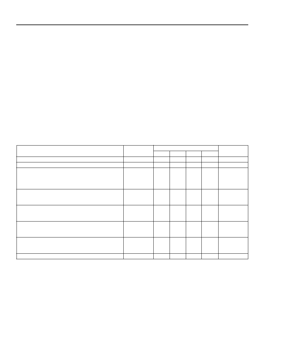
Table 2.
ORCA Series 3 System Performance
1. Implemented using 8 x 1 multiplier mode (unpipelined), register-to-register, two 8-bit inputs, one 16-bit output.
2. Implemented using two 32 x 12 ROMs and one 12-bit adder, one 8-bit input, one xed operand, one 16-bit output.
3. Implemented using 8 x 1 multiplier mode (fully pipelined), two 8-bit inputs, one 16-bit output (7 of 15 PFUs contain only pipelining registers).
4. Implemented using 32 x 4 RAM mode with read data on 3-state buffer to bidirectional read/write bus.
5. Implemented using 32 x 4 dual-port RAM mode.
6. Implemented in one partially occupied SLIC with decoded output set up to CE in same PLC.
7. Implemented in ve partially occupied SLICs.
Parameter
# PFUs
Speed
Unit
-4
-5
-6
-7
16-bit Loadable Up/Down Counter
2
78
102
131
168
MHz
16-bit Accumulator
2
78
102
131
168
MHz
8 x 8 Parallel Multiplier:
Multiplier Mode, Unpipelined1
ROM Mode, Unpipelined2
Multiplier Mode, Pipelined3
11.5
8
15
19
51
76
25
66
104
30
80
127
38
102
166
MHz
32 x 16 RAM (synchronous):
Single-port, 3-state Bus4
Dual-port5
4
97
127
166
151
203
192
253
MHz
128 x 8 RAM (synchronous):
Single-port, 3-state Bus4
Dual-port5
8
88
116
139
176
MHz
8-bit Address Decode (internal):
Using Softwired LUTs
Using SLICs6
0.25
0
4.87
2.35
3.66
1.82
2.58
1.23
2.03
0.99
ns
32-bit Address Decode (internal):
Using Softwired LUTs
Using SLICs7
2
0
16.06
6.91
12.07
5.41
9.01
4.21
7.03
3.37
ns
36-bit Parity Check (internal)
2
16.06
12.07
9.01
7.03
ns
Select
devices
have
been
discontinued.
See
Ordering
Information
section
for
product
status.
相關(guān)PDF資料 |
PDF描述 |
|---|---|
| OR3T307S240-DB | FPGA, 196 CLBS, 48000 GATES, PQFP240 |
| OR3T556PS240-DB | FPGA, 324 CLBS, 80000 GATES, PQFP240 |
| OR3T806PS240-DB | FPGA, 484 CLBS, 116000 GATES, PQFP240 |
| OR3T807PS240-DB | FPGA, 484 CLBS, 116000 GATES, PQFP240 |
| OR3T55-4BA256I | FPGA, 324 CLBS, 40000 GATES, 80 MHz, PBGA256 |
相關(guān)代理商/技術(shù)參數(shù) |
參數(shù)描述 |
|---|---|
| OR3T30-7BA256 | 制造商:AGERE 制造商全稱:AGERE 功能描述:3C and 3T Field-Programmable Gate Arrays |
| OR3T307BA256-DB | 功能描述:FPGA - 現(xiàn)場(chǎng)可編程門陣列 1568 LUT 221 I/O RoHS:否 制造商:Altera Corporation 系列:Cyclone V E 柵極數(shù)量: 邏輯塊數(shù)量:943 內(nèi)嵌式塊RAM - EBR:1956 kbit 輸入/輸出端數(shù)量:128 最大工作頻率:800 MHz 工作電源電壓:1.1 V 最大工作溫度:+ 70 C 安裝風(fēng)格:SMD/SMT 封裝 / 箱體:FBGA-256 |
| OR3T30-7BA256I | 制造商:AGERE 制造商全稱:AGERE 功能描述:3C and 3T Field-Programmable Gate Arrays |
| OR3T30-7BA352 | 制造商:AGERE 制造商全稱:AGERE 功能描述:3C and 3T Field-Programmable Gate Arrays |
| OR3T30-7BA352I | 制造商:AGERE 制造商全稱:AGERE 功能描述:3C and 3T Field-Programmable Gate Arrays |
發(fā)布緊急采購,3分鐘左右您將得到回復(fù)。