- 您現(xiàn)在的位置:買賣IC網(wǎng) > PDF目錄367639 > P11C68-CG (Zarlink Semiconductor Inc.) CMOS/SNOS NVSRAM HIGH PERFORMANCE 8 K x 8 NON-VOLATILE STATIC RAM PDF資料下載
參數(shù)資料
| 型號(hào): | P11C68-CG |
| 廠商: | Zarlink Semiconductor Inc. |
| 英文描述: | CMOS/SNOS NVSRAM HIGH PERFORMANCE 8 K x 8 NON-VOLATILE STATIC RAM |
| 中文描述: | 的CMOS / SNOS非易失性SRAM的高性能8畝× 8非易失性靜態(tài)RAM的 |
| 文件頁數(shù): | 13/17頁 |
| 文件大?。?/td> | 162K |
| 代理商: | P11C68-CG |

P10C68/P11C68
13
OPERATING NOTES
Note: References to NE (bar) should be taken as applying
to P10C68 only and can be ignored for P11C68.
The devices have two separate modes of operation: SRAM
mode and non-volatile mode. In SRAM mode, the memory
operates as an ordinary static RAM. While in non-volatile
mode, data is transferred in parallel from SRAM to EEPROM
or from EEPROM to SRAM.
SRAM READ
The devices perform a read cycle when ever E (bar) and G
(bar) are LOW and NE (bar) and W (bar) are HIGH. The
address specified by the thirteen address pins A
0-12
determine
which of the 8192 data bytes will be accessed. When the
READ is initiated by an address transistion, the outputs will be
valid after a delay of t
AVQV
(READ CYCLE 1).
If the READ is initiated by E (bar) or G (bar), the outputs will
be valid at t
ELQV
or t
GLQV
, whichever is later. (READ CYCLE 2).
The data outputs will repeatedly respond to address changes
within the t
AVQV
access time without the need for transitions on
any control input pins and will remain valid until another
address change or until E (bar) or G (bar) is brought HIGH or
W (bar) or NE (bar) is brought LOW.
SRAM WRITE
A write cycle is performed whenever E (bar) and W (bar)
are LOW and NE (bar) is HIGH. The address inputs must be
stable prior to entering the WRITE cycle and must remain
stable until either E (bar) or W (bar) go HIGH at the end of the
cycle. The data on the eight pins DQ
0-7
, will be written into the
memory location specified by the address inputs if valid t
DVWH
before the end of a W (bar) controlled WRITE or t
DVEH
before
the end of an E (bar) controlled WRITE.
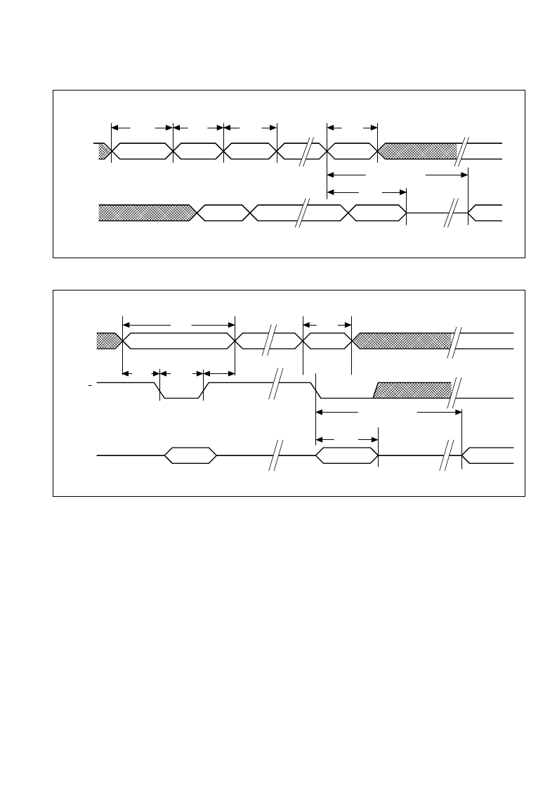
Figure 15. STORE/RECALL cycle 2. E (bar) controlled timing diagram (see notes 22, 25 and 27).
t
SKEW
t
AVAV
t
AVAV
t
AVAV
t
STORE /
t
RECALL
t
AVQZ
INVALID
ADDRESS 1
ADDRESS 2
ADDRESS 6
DATA VALID
DATA VALID
DATA VALID
DATA VALID
HIGH
IMPEDANCE
ADDRESS
DQ
(DATA
OUT)
Figure 14. STORE/RECALL cycle 1. Address controlled timing diagram (see notes 22, 26 and 27).
ADDRESS 1
ADDRESS 6
t
AVAV
t
AVAV
ADDRESS
E
t
ELEH
t
AVEL
t
EHAX
t
STORE /
t
RECALL
DATA VALID
DATA VALID
DATA VALID
HIGH
IMPEDANCE
DQ
(DATA
OUT)
t
ELQZ
相關(guān)PDF資料 |
PDF描述 |
|---|---|
| P11C68-CGDCBS | CMOS/SNOS NVSRAM HIGH PERFORMANCE 8 K x 8 NON-VOLATILE STATIC RAM |
| P11C68-CGDPBS | CMOS/SNOS NVSRAM HIGH PERFORMANCE 8 K x 8 NON-VOLATILE STATIC RAM |
| P11C68-DCBS | CMOS/SNOS NVSRAM HIGH PERFORMANCE 8 K x 8 NON-VOLATILE STATIC RAM |
| P11C68-DPBS | CMOS/SNOS NVSRAM HIGH PERFORMANCE 8 K x 8 NON-VOLATILE STATIC RAM |
| P11C68-IG | CMOS/SNOS NVSRAM HIGH PERFORMANCE 8 K x 8 NON-VOLATILE STATIC RAM |
相關(guān)代理商/技術(shù)參數(shù) |
參數(shù)描述 |
|---|---|
| P11C68-CGDCBS | 制造商:ZARLINK 制造商全稱:Zarlink Semiconductor Inc 功能描述:CMOS/SNOS NVSRAM HIGH PERFORMANCE 8 K x 8 NON-VOLATILE STATIC RAM |
| P11C68-CGDPBS | 制造商:ZARLINK 制造商全稱:Zarlink Semiconductor Inc 功能描述:CMOS/SNOS NVSRAM HIGH PERFORMANCE 8 K x 8 NON-VOLATILE STATIC RAM |
| P11C68-DCBS | 制造商:ZARLINK 制造商全稱:Zarlink Semiconductor Inc 功能描述:CMOS/SNOS NVSRAM HIGH PERFORMANCE 8 K x 8 NON-VOLATILE STATIC RAM |
| P11C68-DPBS | 制造商:ZARLINK 制造商全稱:Zarlink Semiconductor Inc 功能描述:CMOS/SNOS NVSRAM HIGH PERFORMANCE 8 K x 8 NON-VOLATILE STATIC RAM |
| P11C68-IG | 制造商:ZARLINK 制造商全稱:Zarlink Semiconductor Inc 功能描述:CMOS/SNOS NVSRAM HIGH PERFORMANCE 8 K x 8 NON-VOLATILE STATIC RAM |
發(fā)布緊急采購,3分鐘左右您將得到回復(fù)。