- 您現(xiàn)在的位置:買賣IC網(wǎng) > PDF目錄369945 > PA28F008SC-85 (INTEL CORP) BYTE-WIDE SmartVoltage FlashFile MEMORY FAMILY 4, 8, AND 16 MBIT PDF資料下載
參數(shù)資料
| 型號: | PA28F008SC-85 |
| 廠商: | INTEL CORP |
| 元件分類: | PROM |
| 英文描述: | BYTE-WIDE SmartVoltage FlashFile MEMORY FAMILY 4, 8, AND 16 MBIT |
| 中文描述: | 1M X 8 FLASH 3.3V PROM, 85 ns, PDSO44 |
| 封裝: | 13.30 X 28.20 MM, PLASTIC, SOP-44 |
| 文件頁數(shù): | 10/33頁 |
| 文件大?。?/td> | 466K |
| 代理商: | PA28F008SC-85 |
第1頁第2頁第3頁第4頁第5頁第6頁第7頁第8頁第9頁當前第10頁第11頁第12頁第13頁第14頁第15頁第16頁第17頁第18頁第19頁第20頁第21頁第22頁第23頁第24頁第25頁第26頁第27頁第28頁第29頁第30頁第31頁第32頁第33頁

28F008SA
Data Protection
Depending on the application, the system designer
may choose to make the V
PP
power supply switcha-
ble (available only when memory byte writes/block
erases are required) or hardwired to V
PPH
. When
V
PP
e
V
PPL
, memory contents cannot be altered.
The 28F008SA Command User Interface architec-
ture provides protection from unwanted byte write or
block erase operations even when high voltage is
applied to V
PP
. Additionally, all functions are dis-
abled whenever V
CC
is below the write lockout volt-
age V
LKO
, or when RP
Y
is at V
IL
. The 28F008SA
accommodates either design practice and encour-
ages optimization of the processor-memory inter-
face.
The two-step byte write/block erase Command User
Interface write sequence provides additional soft-
ware write protection.
BUS OPERATION
Flash memory reads, erases and writes in-system
via the local CPU. All bus cycles to or from the flash
memory conform to standard microprocessor bus
cycles.
Read
The 28F008SA has three read modes. The memory
can be read from any of its blocks, and information
can be read from the intelligent identifier or Status
Register. V
PP
can be at either V
PPL
or V
PPH
.
The first task is to write the appropriate read mode
command to the Command User Interface (array, in-
telligent
identifier,
or
28F008SA automatically resets to Read Array mode
upon initial device powerup or after exit from deep
powerdown. The 28F008SA has four control pins,
two of which must be logically active to obtain data
at the outputs. Chip Enable (CE
Y
) is the device se-
lection control, and when active enables the select-
ed memory device. Output Enable (OE
Y
) is the data
input/output (DQ
0
–DQ
7
) direction control, and when
active drives data from the selected memory onto
the I/O bus. RP
Y
and WE
Y
must also be at V
IH
.
Figure 10 illustrates read bus cycle waveforms.
Status
Register).
The
Output Disable
With OE
Y
at a logic-high level (V
IH
), the device out-
puts are disabled. Output pins (DQ
0
–DQ
7
) are
placed in a high-impedance state.
Standby
CE
Y
at a logic-high level (V
IH
) places the 28F008SA
in standby mode. Standby operation disables much
of the 28F008SA’s circuitry and substantially reduc-
es device power consumption. The outputs (DQ
0
–
DQ
7
) are placed in a high-impedence state indepen-
dent of the status of OE
Y
. If the 28F008SA is dese-
lected during block erase or byte write, the device
will continue functioning and consuming normal ac-
tive power until the operation completes.
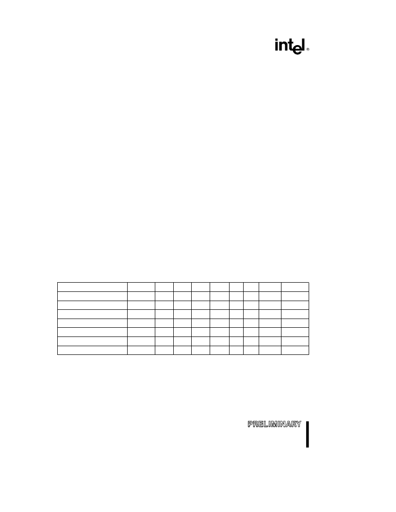
Table 2. Bus Operations
Mode
Notes
RP
Y
CE
Y
OE
Y
WE
Y
A
0
V
PP
DQ
0–7
RY/BY
Y
Read
1,2,3
V
IH
V
IL
V
IL
V
IH
X
X
D
OUT
X
Output Disable
1,2,3
V
IH
V
IL
V
IH
V
IH
X
X
High Z
X
Standby
1,2,3
V
IH
V
IH
X
X
X
X
High Z
X
Deep PowerDown
1,2
V
IL
X
X
X
X
X
High Z
V
OH
Intelligent Identifier (Mfr)
1,2
V
IH
V
IL
V
IL
V
IH
V
IL
X
89H
V
OH
Intelligent Identifier (Device)
1,2
V
IH
V
IL
V
IL
V
IH
V
IH
X
A2H
V
OH
Write
1,2,3,4,5
V
IH
V
IL
V
IH
V
IL
X
X
D
IN
X
NOTES:
1. Refer to DC Characteristics. When V
PP
e
V
PPL
, memory contents can be read but not written or erased.
2. X can be V
IL
or V
IH
for control pins and addresses, and V
PPL
or V
PPH
for V
PP
. See DC Characteristics for V
PPL
and V
PPH
voltages.
3. RY/BY
Y
is V
OL
when the Write State Machine is executing internal block erase or byte write algorithms. It is V
OH
when
the WSM is not busy, in Erase Suspend mode or deep powerdown mode.
4. Command writes involving block erase or byte write are only successfully executed when V
PP
e
V
PPH
.
5. Refer to Table 3 for valid D
IN
during a write operation.
10
相關(guān)PDF資料 |
PDF描述 |
|---|---|
| PA28F008SA-120 | 8-MBIT (1-MBIT x 8) FlashFileTM MEMORY |
| PA28F008SC-120 | BYTE-WIDE SmartVoltage FlashFile MEMORY FAMILY 4, 8, AND 16 MBIT |
| PA34 | POWER OPERATIONAL AMPLIFIERS |
| PA44 | HIGH VOLTAGE POWER OPERATIONAL AMPLIFIER |
| PA7540JI-15 | PA7540 PEEL Array? Programmable Electrically Erasable Logic Array |
相關(guān)代理商/技術(shù)參數(shù) |
參數(shù)描述 |
|---|---|
| PA28F016S5-120 | 制造商:INTEL 制造商全稱:Intel Corporation 功能描述:BYTE-WIDE SMART 5 FlashFile MEMORY FAMILY 4, 8, AND 16 MBIT |
| PA28F016S5-95 | 制造商:INTEL 制造商全稱:Intel Corporation 功能描述:BYTE-WIDE SMART 5 FlashFile MEMORY FAMILY 4, 8, AND 16 MBIT |
| PA28F016SC-120 | 制造商:INTEL 制造商全稱:Intel Corporation 功能描述:BYTE-WIDE SmartVoltage FlashFile⑩ MEMORY FAMILY 4, 8, AND 16 MBIT |
| PA28F016SC-95 | 制造商:INTEL 制造商全稱:Intel Corporation 功能描述:BYTE-WIDE SmartVoltage FlashFile⑩ MEMORY FAMILY 4, 8, AND 16 MBIT |
| PA28F200B5B60 | 制造商:INTEL 制造商全稱:Intel Corporation 功能描述:SMART 5 BOOT BLOCK FLASH MEMORY FAMILY 2, 4, 8 MBIT |
發(fā)布緊急采購,3分鐘左右您將得到回復。