- 您現(xiàn)在的位置:買賣IC網(wǎng) > PDF目錄378039 > PACVGA203 (California Micro Devices Corporation) VGA Port Companion Circuit PDF資料下載
參數(shù)資料
| 型號(hào): | PACVGA203 |
| 廠商: | California Micro Devices Corporation |
| 英文描述: | VGA Port Companion Circuit |
| 中文描述: | VGA端口伴侶電路 |
| 文件頁數(shù): | 1/8頁 |
| 文件大?。?/td> | 168K |
| 代理商: | PACVGA203 |
2004 California Micro Devices Corp. All rights reserved.
12/07/04
430 N. McCarthy Blvd., Milpitas, CA 95035-5112
●
Tel: 408.263.3214
●
Fax: 408.263.7846
●
www.calmicro.com
1
PACVGA203
VGA Port Companion Circuit
Features
Single-chip solution for the VGA port interface
Includes ESD protection, level shifting, and RGB
termination
Seven channels of ESD protection for all VGA port
connector pins, meeting IEC-61000-4-2 Level-4
ESD requirements (8kV contact discharge)
Very low loading capacitance from ESD protection
diodes on VIDEO lines; 4pF typical
75
termination resistors for VIDEO lines
(matched to 1% typ.)
TTL to CMOS level-translating buffers with power-
down mode for HSYNC and VSYNC lines
Bi-directional level shifting N-channel FETs pro-
vided for DDC_CLK & DDC_DATA channels
Compact 24-pin QSOP package
Lead-free version available
Applications
Notebook computers with VGA port
Desktop PCs with VGA port
Product Description
The PACVGA203 incorporates seven channels of ESD
protection for all signal lines commonly found in a VGA
port. ESD protection is implemented with current
steering diodes designed to safely handle the high
surge currents encountered with IEC-61000-4-2 Level-
4 ESD Protection (8kV contact discharge). When a
channel is subjected to an electrostatic discharge, the
ESD current pulse is diverted via the protection diodes
into either the positive supply rail or ground where it
may be safely dissipated. Separate positive supply
rails are provided for the VIDEO, DDC and SYNC
channels to facilitate interfacing with low voltage Video
Controller ICs and provide design flexibility in multi-
supply-voltage environments.
Two non-inverting drivers provide buffering for the
HSYNC and VSYNC signals from the Video Controller
IC (SYNC_IN1, SYNC_IN2). These buffers accept TTL
input levels and convert them to CMOS output levels
that swing between Ground and V
CC
4 (cont’d next
page).
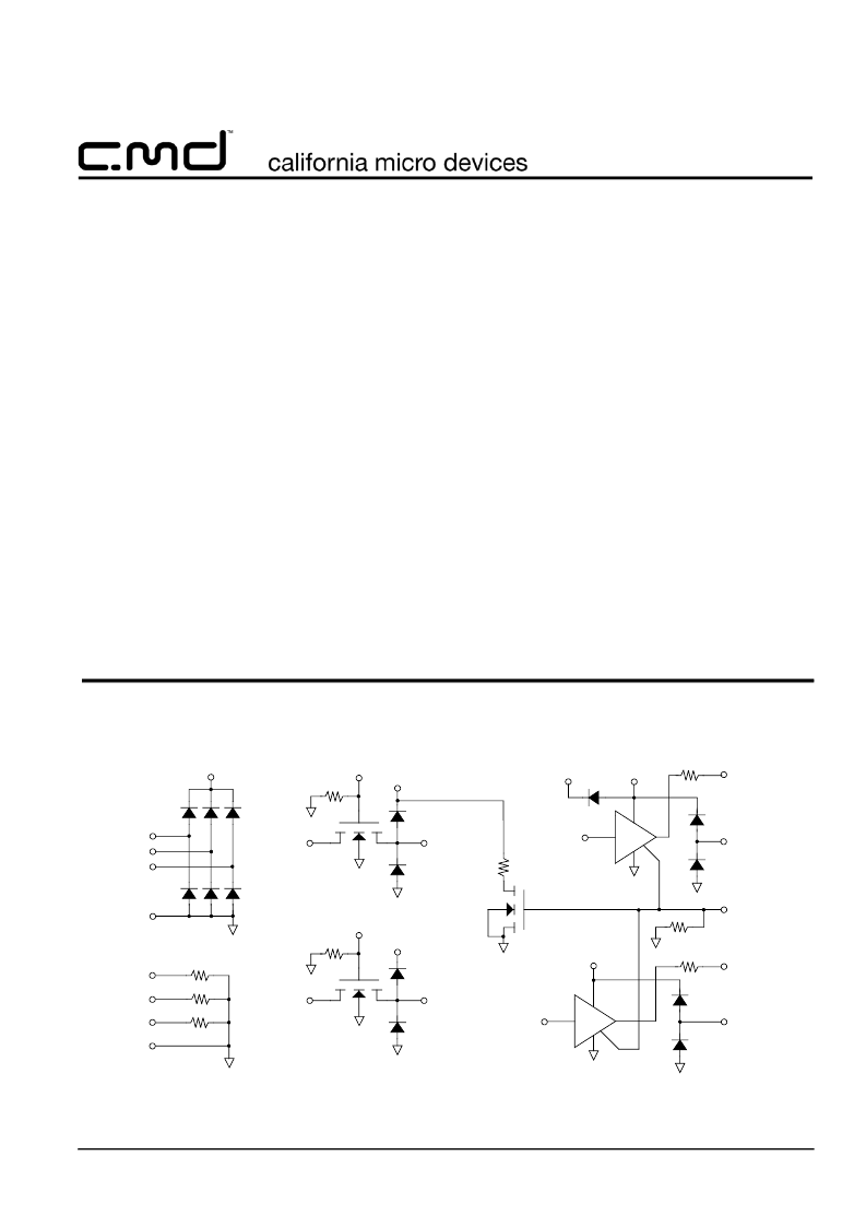
Simplified Electrical Schematic
VIDEO_1
VIDEO_2
VIDEO_3
3
4
5
2
6
V
CC
1
GNDD
GNDD
75
75
75
GNDA
8
9
10
TERM_1
TERM_2
TERM_3
GNDA
7
R
C
V
CC
2
DDC_IN2
17
GNDD
GNDD
GNDD
V
CC
3
18
DDC_OUT2
R
C
V
CC
2
DDC_IN1
16
GNDD
GNDD
GNDD
V
CC
3
14
15
DDC_OUT1
12
GNDD
R
B
19
GNDD
SYNC_IN1
GNDD
V
CC
4
23
SD1
V_BIAS
SYNC_OUT1
PWR_UP
1
13
20
11
R
C
GNDD
21
GNDD
SYNC_IN2
V
CC
4
1
24
SD2
GNDD
SYNC_OUT2
22
R
S
R
S
D1
相關(guān)PDF資料 |
PDF描述 |
|---|---|
| PACVGA203Q | VGA Port Companion Circuit |
| PACVGA203QR | VGA Port Companion Circuit |
| PACZIG128402Q | IEEE 1284 Parallel Port ESD/EMI/Eermination network |
| PACZIG128404Q | IEEE 1284 Parallel Port ESD/EMI/Eermination network |
| PAL22V10Z-25C | EPICE CMOS PROGRAMMABLE ARRAY LOGIC CIRCUITS |
相關(guān)代理商/技術(shù)參數(shù) |
參數(shù)描述 |
|---|---|
| PACVGA203Q | 制造商:CALMIRCO 制造商全稱:California Micro Devices Corp 功能描述:VGA Port Companion Circuit |
| PACVGA203QR | 制造商:CALMIRCO 制造商全稱:California Micro Devices Corp 功能描述:VGA Port Companion Circuit |
| PACZIG1284 | 制造商:未知廠家 制造商全稱:未知廠家 功能描述:PActive? IEEE 1284 Parallel Port ESD/EMI/Termination Network. |
| PACZIG128402Q | 制造商:CALMIRCO 制造商全稱:California Micro Devices Corp 功能描述:IEEE 1284 Parallel Port ESD/EMI/Eermination network |
| PACZIG128404Q | 制造商:CALMIRCO 制造商全稱:California Micro Devices Corp 功能描述:IEEE 1284 Parallel Port ESD/EMI/Eermination network |
發(fā)布緊急采購,3分鐘左右您將得到回復(fù)。