- 您現(xiàn)在的位置:買(mǎi)賣(mài)IC網(wǎng) > PDF目錄378039 > PBD35171N (ERICSSON) Stepper Motor Drive Circuit PDF資料下載
參數(shù)資料
| 型號(hào): | PBD35171N |
| 廠商: | ERICSSON |
| 英文描述: | Stepper Motor Drive Circuit |
| 中文描述: | 步進(jìn)電機(jī)驅(qū)動(dòng)電路 |
| 文件頁(yè)數(shù): | 4/10頁(yè) |
| 文件大小: | 135K |
| 代理商: | PBD35171N |
PBD 3517/1
4
Diagrams
How to use the diagrams:
1.
What is the maximum motor current
in the application
The ambient temperature sets the
maximum allowable power
dissipation in the IC, which
relates to the motor currents and
the duty cycle of the bilevel
function. For PBD 3517/1, without
any measures taken to reduce
the chip temperature via
heatsinks, the power dissipation
vs. temperature follows the curve
in figure 4.
Figures 9 and 10 give the
relationship between motor
currents and their dissipations.
The sum of these power dissipa-
tions must never exceed the
previously-established value, or
life expectancy will be drastically
shortened.
When no bilevel or voltage
doubling is utilized, the maximum
motor current can be found
directly in figure 9.
2.
How to choose timing components.
Figure 7 shows the relationship
between C
, R
, and t
. Care
must be taken to keep the t
time
short, otherwise the current in the
winding will rise to a value many
times the rated current, causing
an overheated IC or motor.
3.
What is the maximum t
On
pulse-width
at a given frequency
Figure 8 shows the relationship
between duty cycle, pulse width,
and step frequency. Check
specifications for the valid
operating area.
4.
Figures 4, 5 and 6 show typical
saturation voltages vs. output current
levels for different output transistors.
5.
Shaded areas represent operating
conditions outside the safe operating
area.
Figure 7. Typical I
vs. V
CE Sat
. “Zero
output” saturation.
Figure 8. Typical t
vs. C
/R
. Output
pulse width vs. capacitance/resistance.
Figure 9. Typical t
vs. f
/dc. Output pulse
width vs. step frequency/duty cycle.
Figure 10. Typical P
vs. I
. Power
dissipation without second-level supply
(includes 2 active outputs = FULL STEP).
Figure 11. Typical P
vs. I
. Power
dissipation in the bilevel pulse when
raising to the I
I
value. One active output.
Figure 12 . Motor Current 1
p
.
T
A
= +25
°
C
10
8
6
4
2
00
0.2
0.4
1.0
0.8
0.6
Output Current [A]
Output Voltage [V]
1
10
-1
10
-6
0.01
0.1
1
1000
100
10
Output Pulse Width [s]
Ct Capacitance [nF]
10
-2
10
-3
10
-4
10
-5
T
A
= +25
°
C
R =10M
R =100k
R =10k
R =1k
1
10
-1
10
-6
0.001
0.01
0.1
100
10
1
Output Pulse Width [s]
fs Step frequency [kHz]
10
-2
10
-3
10
-4
10
-5
T
A
= +25
°
C
50%
25%
Duycyke
100%
01%
1%
10%
0.5
0.4
0.3
0.2
0.1
00
0.2
0.4
1.0
0.8
0.6
Output Current [A]
Power Dissipation [W]
T
A
= +25
°
C
(II = 0)
-0.5
-0.4
-0.3
-0.2
-0.1
00
0.2
0.4
1.0
0.8
0.6
Output Current [A]
Power Dissipation [W]
T
A
= +25
°
C
(Ip = 0)
10%
50%
100%
350
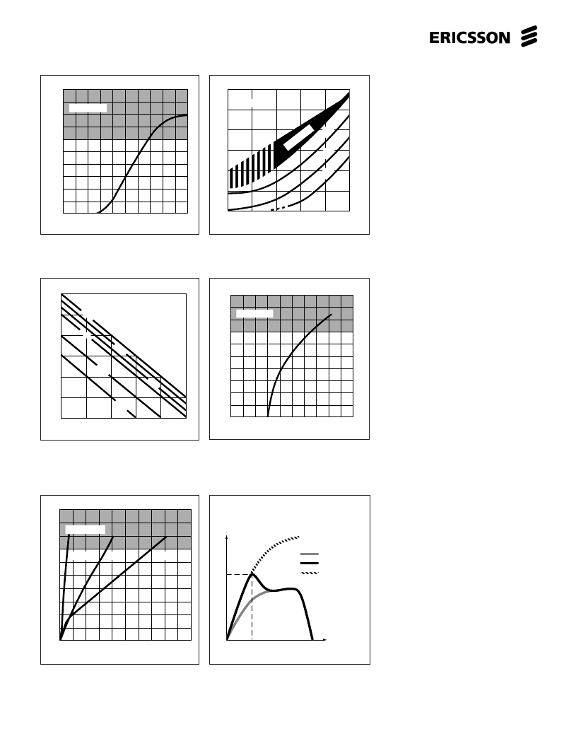
Motor Current [mA]
t
ON
Time
Normal
Bilevel
Bilevel without
time limit
相關(guān)PDF資料 |
PDF描述 |
|---|---|
| PBD35171SO | Stepper Motor Drive Circuit |
| PBD3534 | DTMF Generator |
| PBL3762 | Subcriber Line Interface Circuit |
| PBL3764 | SUBSCRIBER LINE INTERFACE CIRCUIT |
| PBL3770AQNS | ER 3C 3#12 PIN RECP WALL |
相關(guān)代理商/技術(shù)參數(shù) |
參數(shù)描述 |
|---|---|
| PBD35171SO | 制造商:ERICSSON 制造商全稱:Ericsson 功能描述:Stepper Motor Drive Circuit |
| PBD3517N | 制造商:未知廠家 制造商全稱:未知廠家 功能描述:Industrial Control IC |
| PBD3534 | 制造商:ERICSSON 制造商全稱:Ericsson 功能描述:DTMF Generator |
| PBD3535 | 制造商:STMICROELECTRONICS 制造商全稱:STMicroelectronics 功能描述:DTMF Generator |
| PBD3535N | 制造商:未知廠家 制造商全稱:未知廠家 功能描述:Tone Telephone Dialer |
發(fā)布緊急采購(gòu),3分鐘左右您將得到回復(fù)。