- 您現(xiàn)在的位置:買賣IC網(wǎng) > PDF目錄378039 > PBD35171SO (ERICSSON) Stepper Motor Drive Circuit PDF資料下載
參數(shù)資料
| 型號: | PBD35171SO |
| 廠商: | ERICSSON |
| 英文描述: | Stepper Motor Drive Circuit |
| 中文描述: | 步進(jìn)電機(jī)驅(qū)動電路 |
| 文件頁數(shù): | 7/10頁 |
| 文件大?。?/td> | 135K |
| 代理商: | PBD35171SO |
PBD 3517/1
7
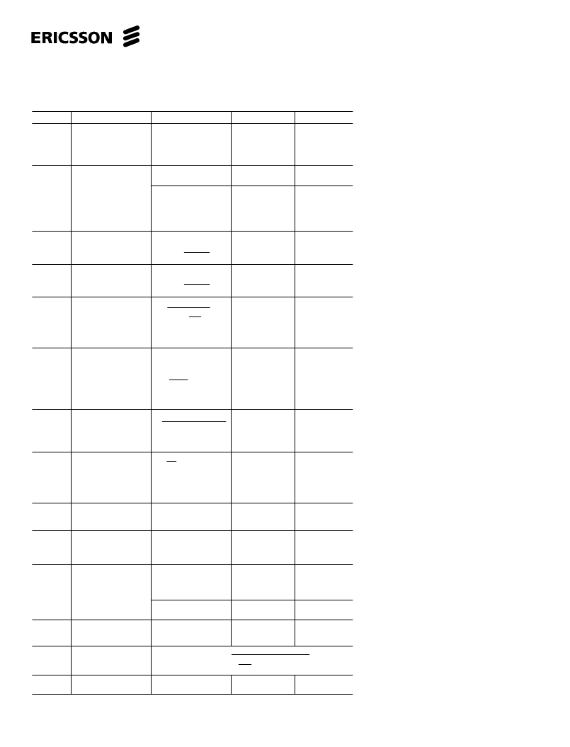
Purpose of external components
For figures 14 and 15. Note that “Larger than …” is normally the vice versa of “Smaller
than … .”
Component Purpose
Value
Larger than value Smaller than value
D1, D2
Passes low power to
motor and prevents
high power from
shorting through low
power supply
If = 1A
1N4001, UF4001
Increases price
Decreases max
current capability
D3 … D6
Inductive current
supressor
Increases price
Decreases current
turn-off capability
trr = 100nS
e.g.
BYV27
UF4001
RGPP10G
RGPP30D
Slows down turn-
off time. Voltage
at anode might
exceed voltage
breakdown
Speeds up turn-
off time.
R1
Base drive current
limitter
R = 20ohm
2
Slows down Q1’s
turn-on and Q4’s
turn-off time.
Speeds up Q1’s
turn-on and Q4’s
turn-off time.
R2, R3
Base discharge resistor R = 240ohm
2
Slows down Q1’s
turn-off and Q4’s
turn-on time.
Speeds up Q1’s
turn-off and Q4’s
turn-on time.
R4 … R7
External transistor base
driver
Vmm- Vbe- Ve
I4 -
)
R12
(
R =
P > (I4)2 R4
Check hfe.
Decreases ext.
transistor ICmax.
Lowers 3517
power dissipation.
Increases ext.
transistor IC max.
Increases 3517
power dissipation.
R8, R9
A, B pull-up
resistors
R = 5ohm @ pull-up
voltage = 5V.
(VCC)2
P =
R
Increases noise
sensitivity, worse
logic-level
definition
Increases noise
immunity, better
logic-level
definition.
Less stress on A,
B output
transistors
Stress on A, B
output
transistors.
R10, R11
Limit max. motor
current. Resistors may
be omitted. (Check
motor specifications
first.)
Vmm-VMotor-VCESat
R =
IMotor max
Decreases motor
current.
Increases motor
current.
R12 … R15 External transistor base
discharge.
Vbe
I12
R =
a 15W
P > Vbe I12
Slows down
external transistor
turn-off time.
Lowers 3517
power dissipation
Speeds up
external transistor
turn-off time.
Increases 3517
power dissipation
RT, CT
Sets LA and LB on time
when triggered by
STEP.
R = 47kohm, C = 10nf
P < 250mW
Increases on time. Decreases on time.
C1, C2
Stores the doubling
voltage.
C = 100
μ
F
VC
≥
45V
Increases effective
on-time during
voltage doubling
Decreases
effective on-time
during voltage
doubling.
C3 … C5
Filtering of supply-
voltage ripple and take-
up of energy feedback
from D3 … D6
C
μ
F
Increases price,
better filtering,
decreases risk of
IC breakdown
Decreases price,
more compact
solution.
VRated>Vmm,Vss or VccIncreases price
Risk for capacitor
breakdown.
Q1, Q2
Activation transistor of
voltage doubling.
IC as motor requires.
Increases price.
Decreases max Im
during voltage
doubling.
)
Q3, Q4
Charging of voltage
doubling capacitor
Q5 … Q8
Motor current drive
transistor.
PNP power trans.
Increases max
current capability.
Decreases max
current capability.
If = 1A
Vmm
R1 + R2
P = R1
)
)
Vmm
R1 + R2
P = R1
Vbe
(Vmm- Vf -VCE) C1
IC=
(
fStep
- 0.55 RT CT
1
IC as motor requires.
10
≥
INH — Inhibit
A HIGH level on the INH input,turns off all
phase outputs to reduce current
consumption.
Reset
An internal Power-On Reset circuit
connected to V
resets the phase logic
and inhibits the outputs during power up,
to prevent false stepping.
Output Stages
The output stage consists of four open-
collector transistors. The second high-
voltage supply contains Darlington
transistors.
Phase Outputs
The phase outputs are connected directly
to the motor as shown in figure 14.
Bilevel Technique
The bilevel pulse generator consists of
two monostables with a common RC
network.
The internal phase logic generates a
trigger pulse every time the phase
changes state. The pulse triggers its own
monostable which turns on the output
transistors for a precise period of time:
t
On
= 0.55 C
T
R
T
.
See pulse diagrams, figures 16 through
20.
Bipolar Phase Logic Output
The
and
outputs are generated
from the phase logic and inform an
external device if the A phase or the B
phase current is internally inhibited.
These outputs are intended to support if it
is legal to correctly go from a half-step
mode to a full-step mode without loosing
positional information.
The PBD 3517/1 can act as a controller
IC for 2 driver ICs, the PBL 3770A. Use
P
A1
and P
for phase control, and
and
B
for I
0
and I
1
control of current turn-off.
Applications Information
Logic inputs
If any of the logic inputs are left open, the
circuit will treat it as a high-level input.
Unused inputs should be connected to
proper voltage levels in order to get the
highest noise immunity.
Phase outputs
相關(guān)PDF資料 |
PDF描述 |
|---|---|
| PBD3534 | DTMF Generator |
| PBL3762 | Subcriber Line Interface Circuit |
| PBL3764 | SUBSCRIBER LINE INTERFACE CIRCUIT |
| PBL3770AQNS | ER 3C 3#12 PIN RECP WALL |
| PBL3770AQNT | High Performance Stepper Motor Drive Circuit |
相關(guān)代理商/技術(shù)參數(shù) |
參數(shù)描述 |
|---|---|
| PBD3517N | 制造商:未知廠家 制造商全稱:未知廠家 功能描述:Industrial Control IC |
| PBD3534 | 制造商:ERICSSON 制造商全稱:Ericsson 功能描述:DTMF Generator |
| PBD3535 | 制造商:STMICROELECTRONICS 制造商全稱:STMicroelectronics 功能描述:DTMF Generator |
| PBD3535N | 制造商:未知廠家 制造商全稱:未知廠家 功能描述:Tone Telephone Dialer |
| PBD3545/1 | 制造商:未知廠家 制造商全稱:未知廠家 功能描述:IC-SINK DRIVER |
發(fā)布緊急采購,3分鐘左右您將得到回復(fù)。