- 您現(xiàn)在的位置:買賣IC網 > PDF目錄378039 > PBL3771-1 (ERICSSON) KPT 10C 10#20 SKT PLUG PDF資料下載
參數資料
| 型號: | PBL3771-1 |
| 廠商: | ERICSSON |
| 英文描述: | KPT 10C 10#20 SKT PLUG |
| 中文描述: | 精密步進電機驅動器 |
| 文件頁數: | 7/8頁 |
| 文件大?。?/td> | 154K |
| 代理商: | PBL3771-1 |
PBL 3771/1
7
P
D
(W)
0
.10
.20
.30
I
M
(A)
.40
.50
.60
0
1.0
2.0
3.0
V
MM
= 14V
V
MM
= 36V
General
Phase inputs.
A logic HIGH on a Phase
input gives positive current flowing out
from M
into M
. A logic LOW gives a
current in the opposite direction.
Slow/fast current decay.
A logic HIGH
on the CD input gives slow current
decay, a logic LOW gives fast current
decay.
Heat sinking.
Soldering the four center
pins onto a free PCB copper area of 20
cm
2
(approx. 1.8" x 1.8", copper foil
thickness = 35
μ
m) permits the circuit to
operate with a maximum of 320 mA
output current, both channels driving, at
ambient temperatures up to +70
°
C.
Consult figures 12 and 13 in order to
determine the necessary copper area for
heat sinking if higher currents are
required.
Thermal shutdown.
The circuit is
equipped with a thermal shutdown
function that reduces the output current
at chip temperatures above +160
°
C.
Operating temperature.
The max re-
commended operating temperature is
125
°
C. This gives an estimated lifelength
of about 5 years at continous drive, A
change of
±
10
°
would increase/decrease
the lifelength of the circuit with about 5
years.
V
d
(V)
0
.10
.20
.30
I
M
(A)
.40
.50
.60
0
.2
.4
.6
.8
1.0
T
j
= 25
°
C
T
j
= 125
°
C
T
j
= 25
°
C
T
j
= 125
°
C
V
CE Sat
(V)
0
.10
.20
.30
I
M
(A)
.40
.50
.60
.2
.4
.6
.8
1.0
1.2
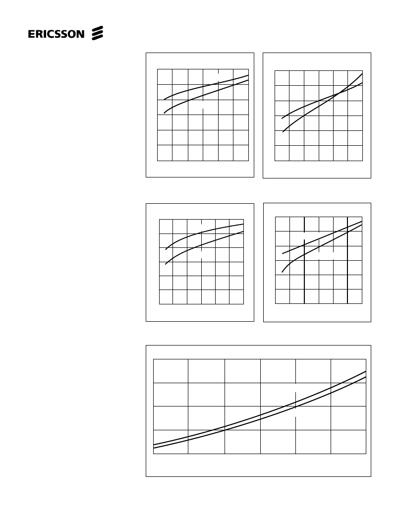
Figure 9. Typical source saturation
voltage vs. output current.
Figure 8. Typical upper diode voltage
drop vs. recirculating current.
Figure 10. Typical lower diode voltage
drop vs. recirculating current.
Figure 11 Typical sink saturation voltage
vs. output current.
V
d
(V)
0
.10
.20
.30
I
M
(A)
.40
.50
.60
0
.2
.4
.6
.8
1.0
T
j
= 25
°
C
T
j
= 125
°
C
.2
.4
.6
.8
1.0
V
CE Sat
(V)
0
.10
.20
.30
I
M
(A)
.40
.50
.60
T
j
= 25
°
C
T
j
= 125
°
C
Figure 12. Power dissipation vs. motor current, both channels driven, T
a
= 25
°
C.
Max allow power dis
相關PDF資料 |
PDF描述 |
|---|---|
| PBL37711 | KPTC 10C 10#20 SKT PLUG |
| PBL37711N | KPTC 3C 3#16 PIN PLUG |
| PBL37711QN | KPTC 3C 3#16 PIN PLUG |
| PBL37711SO | KPTC 3C 3#16 SKT PLUG |
| PBL3771N | CONNECTOR GERMAN |
相關代理商/技術參數 |
參數描述 |
|---|---|
| PBL37711N | 制造商:ERICSSON 制造商全稱:Ericsson 功能描述:Precision Stepper Motor Driver |
| PBL37711QN | 制造商:ERICSSON 制造商全稱:Ericsson 功能描述:Precision Stepper Motor Driver |
| PBL37711SO | 制造商:ERICSSON 制造商全稱:Ericsson 功能描述:Precision Stepper Motor Driver |
| PBL3771N | 制造商:ERICSSON 制造商全稱:Ericsson 功能描述:Precision Stepper Motor Driver |
| PBL3771QN | 制造商:ERICSSON 制造商全稱:Ericsson 功能描述:Precision Stepper Motor Driver |
發(fā)布緊急采購,3分鐘左右您將得到回復。