- 您現(xiàn)在的位置:買賣IC網(wǎng) > PDF目錄367800 > PC812B NPN-OUTPUT DC-INPUT OPTOCOUPLER PDF資料下載
參數(shù)資料
| 型號: | PC812B |
| 英文描述: | NPN-OUTPUT DC-INPUT OPTOCOUPLER |
| 中文描述: | npn型輸出DC -輸入光耦合器 |
| 文件頁數(shù): | 1/5頁 |
| 文件大小: | 75K |
| 代理商: | PC812B |
PC812
PC812
I
Features
1. High noise reduction
(Common mode rejection voltage
V
CM
R
L
= 470
, V
np
= 100mV )
2. High current transfer ratio
(CTR : MIN. 90% at I
F
= 5mA, V
CE
= 5V)
3. High isolation voltage between input and
output (V
iso
: 5 000V
rms
)
4. Compact dual-in-line package
I
Applications
1. Motor-control circuits
2. Computer terminals
3. System appliances, measuring instruments
4. Signal transmission between circuits of
different potentials and impedances
*3 For 10 seconds
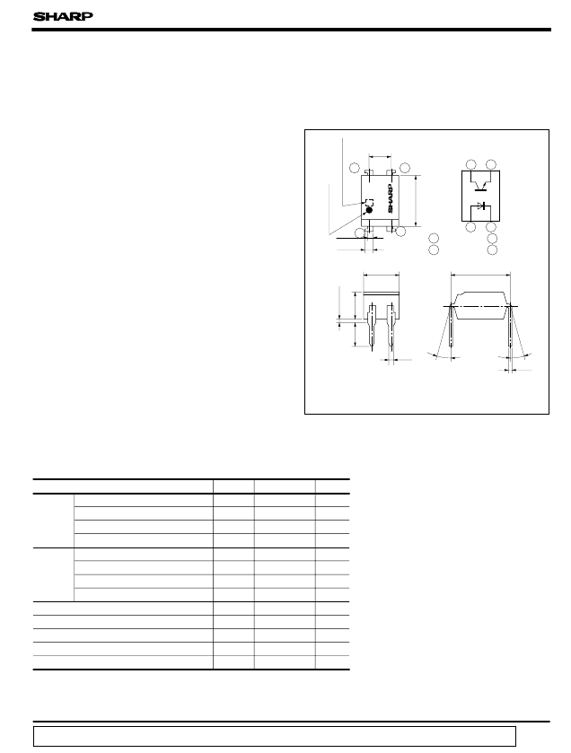
( Unit : mm)
I
Absolute Maximum Ratings
Parameter
Symbol
I
F
I
FM
V
R
P
V
CEO
V
ECO
I
C
P
C
P
tot
V
iso
T
opr
T
stg
T
sol
Rating
50
1
6
70
35
6
50
150
200
5 000
Unit
mA
A
V
mW
V
V
mA
mW
mW
V
rms
Input
Forward current
*1
Peak forward current
Reverse voltage
Power dissipation
Collector-emitter voltage
Emitter-collector voltage
Collector current
Collector power dissipation
Total power dissipation
Output
*2
Isolation voltage
Operating temperature
Storage temperature
*3
Soldering temperature
- 30 to + 100
- 55 to + 125
260
C
C
C
*1 Pulse width<=100
μ
s, Duty ratio : 0.001
*2 40 to 60%RH, AC for 1 minute
data books, etc. Contact SHARP in order to obtain the latest version of the device specification sheets before using any SHARP's device.
”
“
In the absence of confirmation by device specification sheets, SHARP takes no responsibility for any defects that occur in equipment using any of SHARP's devices, shown in catalogs,
θ
0.26
±
0.1
θ
A
C
P
Internal connection
diagram
4
3
1
2
3
4
2
3 Emitter
4 Collector
1
0
1 Anode
2 Cathode
Photocoupler
(T
a
= 25C)
High Noise Resistance Type
I
Outline Dimensions
4.58
±
0.5
: TYP. 1.5kV at d
V
/dt= 2kV/
μ
s,
7.62
±
0.3
θ
=
0 to 13
6
±
2.54
±
0.25
0.9
±
0.2
1.2
±
0.3
3
±
3
±
0
0.5
±
0.1
相關(guān)PDF資料 |
PDF描述 |
|---|---|
| PC812A | |
| PC812C | NPN-OUTPUT DC-INPUT OPTOCOUPLER |
| PC812 | High Noise Resistance Type Photocoupler |
| PC813A | |
| PC813 | AC Input Type & High Noise Reduction Type Photocoupler |
相關(guān)代理商/技術(shù)參數(shù) |
參數(shù)描述 |
|---|---|
| PC812C | 制造商:SHARP 制造商全稱:Sharp Electrionic Components 功能描述:High Noise Resistance Type Photocoupler |
| PC812X1NIPJF | 制造商:Sharp Microelectronics Corporation 功能描述: |
| PC813 | 制造商:Panasonic Industrial Company 功能描述:SENSOR |
| PC813A | 制造商:未知廠家 制造商全稱:未知廠家 功能描述: |
| PC814 | 制造商:SHARP 制造商全稱:Sharp Electrionic Components 功能描述:DEVICE SPECIFICATION FOR PHOTOCOUPLER |
發(fā)布緊急采購,3分鐘左右您將得到回復(fù)。