- 您現(xiàn)在的位置:買賣IC網(wǎng) > PDF目錄369960 > PDI1394L21BE (NXP SEMICONDUCTORS) 1394 full duplex AV link layer controller PDF資料下載
參數(shù)資料
| 型號(hào): | PDI1394L21BE |
| 廠商: | NXP SEMICONDUCTORS |
| 元件分類: | 微控制器/微處理器 |
| 英文描述: | 1394 full duplex AV link layer controller |
| 中文描述: | 1 CHANNEL(S), 400M bps, SERIAL COMM CONTROLLER, PQFP100 |
| 封裝: | 14 X 14 MM, 1.40 MM HEIGHT, PLASTIC, SOT-407-1, LQFP-100 |
| 文件頁數(shù): | 38/42頁 |
| 文件大?。?/td> | 233K |
| 代理商: | PDI1394L21BE |
第1頁第2頁第3頁第4頁第5頁第6頁第7頁第8頁第9頁第10頁第11頁第12頁第13頁第14頁第15頁第16頁第17頁第18頁第19頁第20頁第21頁第22頁第23頁第24頁第25頁第26頁第27頁第28頁第29頁第30頁第31頁第32頁第33頁第34頁第35頁第36頁第37頁當(dāng)前第38頁第39頁第40頁第41頁第42頁

Philips Semiconductors
Preliminary data
PDI1394P23
2-port/1-port 400 Mbps physical layer interface
2001 Sep 06
38
The sequence of events for initialization of the PHY-LLC interface
when the interface is in the differentiated mode of operation (ISO
terminal is low) is as follows:
1. LPS reasserted. After the interface has been in the reset or
disabled state for at least the minimum T
RESTORE
time, the LLC
causes the interface to be initialized and restored to normal
operation by re-activating the LPS signal. (In the above diagram,
the interface is shown in the disabled state with SYSCLK
high-impedance inactive. However, the interface initialization
sequence described here is also executed if the interface is
merely reset but not yet disabled.)
2. SYSCLK activated. If the interface is disabled, the PHY
re-activates its SYSCLK output when it detects that LPS has
been reasserted. SYSCLK will be restored within 60 ns. The
PHY commences SYSCLK activity by driving the SYSCLK
output low for half a cycle. Thereafter, the SYSCLK output is a
50% duty cycle square wave with a frequency of 49.152 MHz
+100 ppm (period of 20.345 ns). Upon the first full cycle of
SYSCLK, the PHY drives the CTL and D terminals low for one
cycle. The LLC is also required to drive its CTL, D, and LREQ
outputs low during one of the first six cycles of SYSCLK (in the
above diagram, this is shown as occurring in the first SYSCLK
cycle).
3. Receive indicated. Upon the eighth SYSCLK cycle following
reassertion of LPS, the PHY asserts the Receive state on the
CTL lines and the data-on indication (all ones) on the D lines for
one or more cycles (because the interface is in the differentiated
mode of operation, the CTL and D lines will be in the
high-impedance state after the first cycle).
4. Initialization complete. The PHY asserts the Idle state on the
CTL lines and logic 0 on the D lines. This indicates that the
PHY-LLC interface initialization is complete and normal
operation may commence. The PHY will now accept requests
from the LLC via the LREQ line.
T
CLK_ACTIVATE
CTL0
LPS
SV01815
ISO
SYSCLK
D0 – D7
LREQ
(high)
(c)
7 cycles
(b)
CTL1
(a)
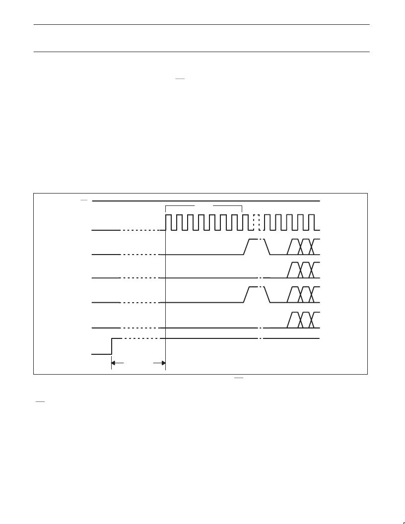
Figure 25.
Interface Initialization, ISO High
The sequence of events for initialization of the PHY-LLC interface
when the interface is in the non-differentiated mode of operation
(ISO terminal is high) is as follows:
1. LPS reasserted. After the interface has been in the reset or
disabled state for at least the minimum T
RESTORE
time, the LLC
causes the interface to be initialized and restored to normal
operation by reasserting the LPS signal. (In the above diagram,
the interface is shown in the disabled state with SYSCLK low
inactive. However, the interface initialization sequence described
here is also executed if the interface is merely reset but not yet
disabled.)
2. SYSCLK activated. If the interface is disabled, the PHY
re-activates its SYSCLK output when it detects that LPS has
been reasserted. SYSCLK will be restored within 60 ns. The
SYSCLK output is a 50% duty cycle square wave with a
frequency of 49.152 MHz +100 ppm (period of 20.345 ns).
During the first seven cycles of SYSCLK, the PHY continues to
drive the CTL and D terminals low. The LLC is also required to
drive its CTL and D outputs low for one of the first six cycles of
SYSCLK but to otherwise place its CTL and D outputs in a
high-impedance state. The LLC continues to drive its LREQ
output low during this time.
3. Receive indicated. Upon the eighth SYSCLK cycle following
reassertion of LPS, the PHY asserts the Receive state on the
CTL lines and the data-on indication (all ones) on the D lines for
one or more cycles.
4. Initialization complete. The PHY asserts the Idle state on the
CTL lines and logic 0 on the D lines. This indicates that the
PHY-LLC interface initialization is complete and normal
operation may commence. The PHY will now accept requests
from the LLC via the LREQ line.
相關(guān)PDF資料 |
PDF描述 |
|---|---|
| PDI1394L21BP | 1394 full duplex AV link layer controller |
| PDL-TTL-7-1 | Programmable Delay Line |
| PDL-TTL-7-14 | Programmable Delay Line |
| PDL-TTL-7-15 | Programmable Delay Line |
| PDL-TTL-7-2 | Programmable Delay Line |
相關(guān)代理商/技術(shù)參數(shù) |
參數(shù)描述 |
|---|---|
| PDI1394L21BP | 制造商:PHILIPS 制造商全稱:NXP Semiconductors 功能描述:1394 full duplex AV link layer controller |
| PDI1394L40 | 制造商:PHILIPS 制造商全稱:NXP Semiconductors 功能描述:1394 enhanced AV link layer controller |
| PDI1394L40BE | 制造商:NXP Semiconductors 功能描述:1 CHANNEL(S), 400M BPS, SERIAL COMM CONTROLLER, PQFP144 |
| PDI1394L40BE,518 | 功能描述:視頻 IC 1394 A/V LINK LAYER RoHS:否 制造商:Fairchild Semiconductor 工作電源電壓:5 V 電源電流:80 mA 最大工作溫度:+ 85 C 封裝 / 箱體:TSSOP-28 封裝:Reel |
| PDI1394L40BE,551 | 制造商:NXP Semiconductors 功能描述:1394 A/V LINK LAYER - Trays |
發(fā)布緊急采購,3分鐘左右您將得到回復(fù)。