- 您現(xiàn)在的位置:買賣IC網(wǎng) > PDF目錄369983 > PDU10256-6C5 Delay Line PDF資料下載
參數(shù)資料
| 型號: | PDU10256-6C5 |
| 英文描述: | Delay Line |
| 中文描述: | 延遲線 |
| 文件頁數(shù): | 2/5頁 |
| 文件大小: | 69K |
| 代理商: | PDU10256-6C5 |

PDU1016H
Doc #97044
DATA DELAY DEVICES, INC.
2
Powered by ICminer.com Electronic-Library Service CopyRight 2003
APPLICATION NOTES
ADDRESS UPDATE
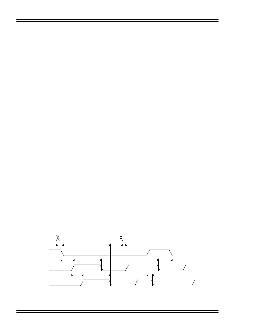
The PDU1016H is a memory device. As such,
special precautions must be taken when
changing the delay address in order to prevent
spurious output signals. The timing restrictions
are shown in Figure 1.
After the last signal edge to be delayed has
appeared on the OUT pin, a minimum time,
T
OAX
, is required before the address lines can
change. This time is given by the following
relation:
T
OAX
= max { (A
i
- A
i-1
) * T
INC
, 0 }
where A
i-1
and A
i
are the old and new address
codes, respectively. Violation of this constraint
may, depending on the history of the input signal,
cause spurious signals to appear on the OUT
pin. The possibility of spurious signals persists
until the required T
OAX
has elapsed.
A similar situation occurs when using the ENB
signal to disable the output while IN is active. In
this case, the unit must be held in the disabled
state until the device is able to “clear” itself. This
is achieved by holding the ENB signal high and
the IN signal low for a time given by:
T
DISH
= A
i
* T
INC
Violation of this constraint may, depending on
the history of the input signal, cause spurious
signals to appear on the OUT pin. The
possibility of spurious signals persists until the
required T
DISH
has elapsed.
INPUT RESTRICTIONS
There are three types of restrictions on input
pulse width and period listed in the
AC
Characteristics
table. The
recommended
conditions are those for which the delay
tolerance specifications and monotonicity are
guaranteed. The
suggested
conditions are
those for which signals will propagate through the
unit without significant distortion. The
absolute
conditions are those for which the unit will
produce some type of output for a given input.
When operating the unit between the
recommended and absolute conditions, the
delays may deviate from their values at low
frequency. However, these deviations will
remain constant from pulse to pulse if the input
pulse width and period remain fixed. In other
words, the delay of the unit exhibits frequency
and pulse width dependence when operated
beyond the recommended conditions. Please
consult the technical staff at Data Delay Devices
if your application has specific high-frequency
requirements.
Please note that the increment tolerances listed
represent a design goal. Although most delay
increments will fall within tolerance, they are not
guaranteed throughout the address range of the
unit. Monotonicity is, however, guaranteed over
all addresses.
T
DISO
T
OAX
T
AENS
T
ENIS
PW
IN
TD
A
PW
OUT
T
DISH
A3-A0
ENB
IN
OUT
Figure 1: Timing Diagram
A
i-1
A
i
T
AIS
相關(guān)PDF資料 |
PDF描述 |
|---|---|
| PDU10256-6M | Delay Line |
| PDU10256-6MC5 | Delay Line |
| PDU10256-8 | Programmable Delay Line |
| PDU10256-8C5 | Delay Line |
| PDU10256-8M | Delay Line |
相關(guān)代理商/技術(shù)參數(shù) |
參數(shù)描述 |
|---|---|
| PDU10256-6M | 制造商:未知廠家 制造商全稱:未知廠家 功能描述:Delay Line |
| PDU10256-6MC5 | 制造商:未知廠家 制造商全稱:未知廠家 功能描述:Delay Line |
| PDU-10256-7 | 制造商:未知廠家 制造商全稱:未知廠家 功能描述:Programmable Delay Line |
| PDU10256-8 | 制造商:未知廠家 制造商全稱:未知廠家 功能描述:Programmable Delay Line |
| PDU10256-8C5 | 制造商:未知廠家 制造商全稱:未知廠家 功能描述:Delay Line |
發(fā)布緊急采購,3分鐘左右您將得到回復(fù)。