- 您現(xiàn)在的位置:買賣IC網(wǎng) > PDF目錄367929 > PGA207 Micropower single-supply CMOS Instrumentation Amplifier PDF資料下載
參數(shù)資料
| 型號: | PGA207 |
| 元件分類: | 測量放大器 |
| 英文描述: | Micropower single-supply CMOS Instrumentation Amplifier |
| 中文描述: | 微功耗單電源 CMOS 儀表放大器 |
| 文件頁數(shù): | 8/10頁 |
| 文件大小: | 246K |
| 代理商: | PGA207 |
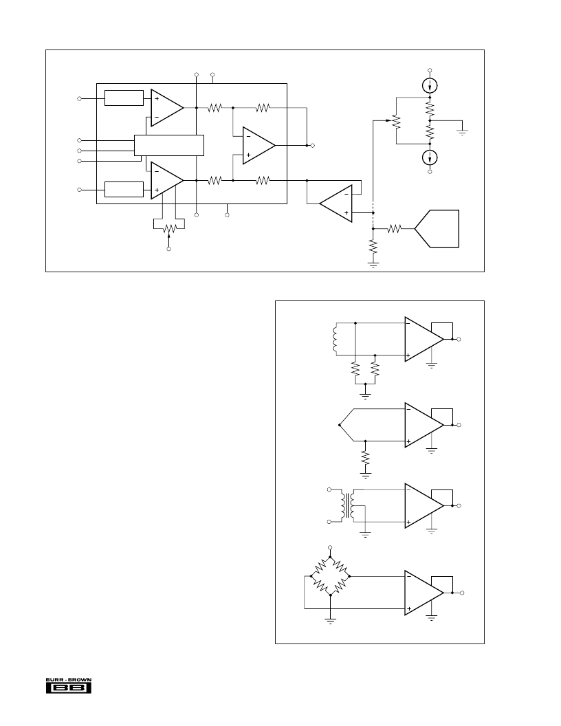
8
PGA206/207
FIGURE 2. Optional Offset Voltage Trim Circuits.
R
1
adjusts the offset of the input amplifiers. Output stage
offset is adjusted with R
2
. A buffer op amp is required in
the output offset adjustment circuit, as shown, to assure
that the Ref pin is driven by a low source impedance. To
adjust for low offset voltage in all gains, first adjust the
input stage offset in the highest gain. Then adjust the
output stage offset (R
2
) in G = 1. Iterate the adjustments for
lowest offset in all gains.
Offset can also be adjusted under processor control with a
D/A converter as shown in Figure 2. The D/A’s output
voltage can be reduced with a resistor divider for better
adjustment resolution, but an op amp buffer following the
divider is required to provide a low source impedance to
the ref terminal. A different offset value is required for
each amplifier gain.
INPUT BIAS CURRENT RETURN PATH
The FET inputs of the PGA206 and PGA207 provide ex-
tremely high input impedance. Still, a path must be provided
for the bias current of each input. Figure 3 shows provisions
for an input bias current path. Without a bias current return
path, the inputs will float to a potential which exceeds the
linear input voltage range and the input amplifiers will
saturate.
If the differential source resistance is low, a bias current
return path can be connected to only one input (see thermo-
couple example in Figure 3). With higher source impedance,
using two resistors provides a balanced input with possible
advantages of lower input offset voltage due to bias current
and better common-mode rejection.
Many sources or sensors inherently provide a path for input
bias current (e.g. the bridge sensor shown in Figure 3).
These applications do not require additional resistor(s) for
proper operation.
FIGURE 3. Providing an Input Bias Current Path.
47k
47k
10k
Microphone,
Hydrophone
etc.
Thermocouple
Center-tap provides
bias current return.
V
R
Bridge
Bias current return
inherrently provided by source.
PGA
PGA
PGA
PGA
A
1
A
2
A
3
12
11
10
10k
10k
10k
10k
7
PGA206
PGA207
Resistors can be substituted
for REF200. Power supply
rejection will be degraded.
Digitally Selected
Feedback Network
6
V
O2
V+
V
O
OPA131
D/A
V+
R
2
10k
100
100
V–
V
REF
5
14
16
4
V
IN
V
IN
–
+
15
A
1
A
0
Digital
Ground
Optional Input Offset Adjustment
13
V+
1
V
O1
9
8
V–
Over-Voltage
Protection
Over-Voltage
Protection
100μA
1/2 REF200
100μA
1/2 REF200
Offset control with
digital/analog converter
Manual output offset trim circuit.
200k
(100k
to 500k
)
R
1
相關(guān)PDF資料 |
PDF描述 |
|---|---|
| PGA207P | Micropower single-supply CMOS Instrumentation Amplifier |
| PGA207PA | Micropower single-supply CMOS Instrumentation Amplifier |
| PGA207U | Micropower single-supply CMOS Instrumentation Amplifier |
| PGA2310PAG4 | Stereo Audio Volume Control |
| PGA2310UAG4 | Stereo Audio Volume Control |
相關(guān)代理商/技術(shù)參數(shù) |
參數(shù)描述 |
|---|---|
| PGA207P | 制造商:BB 制造商全稱:BB 功能描述:High-Speed Programmable Gain INSTRUMENTATION AMPLIFIER |
| PGA207PA | 制造商:BB 制造商全稱:BB 功能描述:High-Speed Programmable Gain INSTRUMENTATION AMPLIFIER |
| PGA207U | 制造商:BB 制造商全稱:BB 功能描述:High-Speed Programmable Gain INSTRUMENTATION AMPLIFIER |
| PGA207UA | 功能描述:儀表放大器 High-Speed Prog Gain RoHS:否 制造商:Texas Instruments 通道數(shù)量: 輸入補償電壓:150 V 可用增益調(diào)整: 最大輸入電阻:10 kOhms 共模抑制比(最小值):88 dB 工作電源電壓:2.7 V to 36 V 電源電流:200 uA 最大工作溫度:+ 125 C 最小工作溫度:- 40 C 封裝 / 箱體:MSOP-8 封裝:Bulk |
| PGA207UA | 制造商:Texas Instruments 功能描述:IC SM AMP INSTRUMENT PROG GAIN |
發(fā)布緊急采購,3分鐘左右您將得到回復(fù)。