- 您現(xiàn)在的位置:買賣IC網(wǎng) > PDF目錄367953 > PI49FCT804TP (Pericom Semiconductor Corp.) Fast CMOS Buffer/Clock Driver PDF資料下載
參數(shù)資料
| 型號(hào): | PI49FCT804TP |
| 廠商: | Pericom Semiconductor Corp. |
| 英文描述: | Fast CMOS Buffer/Clock Driver |
| 中文描述: | 快速CMOS緩沖器/時(shí)鐘驅(qū)動(dòng)器 |
| 文件頁數(shù): | 2/6頁 |
| 文件大小: | 305K |
| 代理商: | PI49FCT804TP |
2
PS7005B 06/26/01
12345678901234567890123456789012123456789012345678901234567890121234567890123456789012345678901212345678901234567890123456789012123456789012
12345678901234567890123456789012123456789012345678901234567890121234567890123456789012345678901212345678901234567890123456789012123456789012
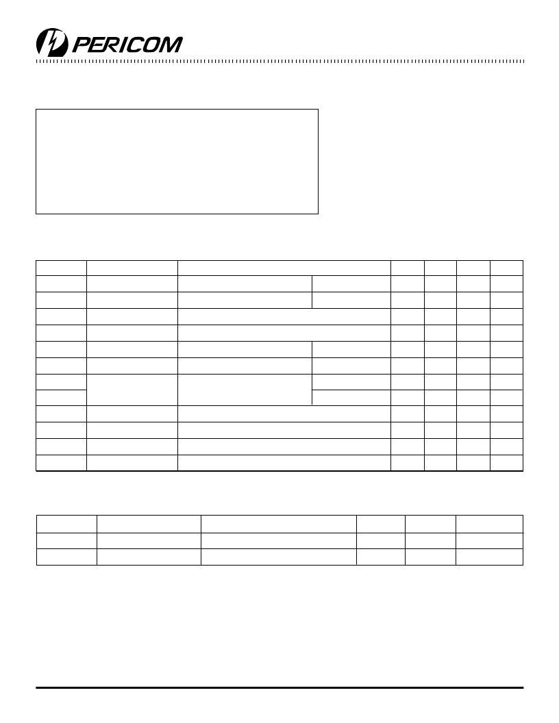
PI49FCT804T
Buffer/Clock Driver
Storage Temperature ........................................................65°C to +150°C
Ambient Temperature with Power Applied ........................... 0°C to +70°C
Supply Voltage to Ground Potential (Inputs & Vcc Only) ..0.5V to +7.0V
Supply Voltage to Ground Potential (Outputs & D/O Only) 0.5V to +7.0V
DC Input Voltage .................................................................0.5V to +7.0V
DC Output Current ..........................................................................120mA
Power Dissipation...............................................................................0.5W
Note:
Stresses greater than those listed under MAXIMUM
RATINGS may cause permanent damage to the device.
This is a stress rating only and functional operation
of the device at these or any other conditions above
those indicated in the operational sections of this
specification is not implied. Exposure to absolute
maximum rating conditions for extended periods may
affect reliability.
DC Electrical Characteristics
(Over the Operating Range, T
A
= 0°C to +70°C, V
CC
= 5.0V ± 5%)
Parameters Description
Test Conditions
(1)
Min.
Typ.
(2)
Max.
Units
V
OH
Output HIGH Voltage
V
CC
= Min., V
IN
= V
IH
or V
IL
I
OH
= 24.0mA
2.4
3.3
V
V
OL
Output LOW Current
V
CC
= Min., V
IN
= V
IH
or V
IL
I
OL
= 64mA
0.3
0.55
V
V
IH
Input HIGH Voltage
Guaranteed Logic HIGH Level
2.0
V
V
IL
Input LOW Voltage
Guaranteed Logic LOW Level
0.8
V
I
IH
Input HIGH Current
V
CC
= Max.
V
IN
= V
CC
1
μA
I
IL
Input LOW Current
V
CC
= Max.
V
IN
= GND
1
μA
I
OZH
I
OZL
High Impedance
Output Current
V
CC
= Max.
V
OUT
= V
CC
V
OUT
= GND
1
μA
μA
1
I
I
Input HIGH Current
V
CC
= Max., V
IN
=V
CC
(Max.)
20
μA
V
IK
Clamp Diode Voltage
V
CC
= Min., I
IN
= 18 mA
0.7
1.2
V
I
OS
Short Circuit Current
V
CC
= Max.
(3)
, V
OUT
= GND
60
120
225
mA
V
H
Input Hysteresis
V
CC
= 5V
200
mV
Capacitance
(T
A
= 25°C, f = 1 MHz)
Parameters
(4)
Description
Test Conditions
Typ.
Max.
Units
C
IN
Input Capacitance
V
IN
= 0V
6
10
pF
C
OUT
Output Capacitance
V
OUT
= 0V
8
12
pF
Notes:
1. For Max. or Min. conditions, use appropriate value specified under Electrical Characteristics for the applicable device type.
2. Typical values are at Vcc = 5.0V, +25°C ambient and maximum loading.
3. Not more than one output should be shorted at one time. Duration of the test should not exceed one second.
4. This parameter is determined by device characterization but is not production tested.
Maximum Ratings
(Above which the useful life may be impaired. For user guidelines, not tested.)
相關(guān)PDF資料 |
PDF描述 |
|---|---|
| PI49FCT807THA | Fast CMOS Clock Driver |
| PI49FCT807TSA | Fast CMOS Clock Driver |
| PI49FCT807TSB | Fast CMOS Clock Driver |
| PI49FCT807TSC | Fast CMOS Clock Driver |
| PI49FCT807ATH | Fast CMOS Clock Driver |
相關(guān)代理商/技術(shù)參數(shù) |
參數(shù)描述 |
|---|---|
| PI49FCT804TQ | 制造商:未知廠家 制造商全稱:未知廠家 功能描述:Four Distributed-Output Clock Driver |
| PI49FCT804TS | 制造商:未知廠家 制造商全稱:未知廠家 功能描述:Four Distributed-Output Clock Driver |
| PI49FCT805AT | 制造商:未知廠家 制造商全稱:未知廠家 功能描述:Clock IC | 5+5 Output Clock Driver with Monitor Output. Industrial Temp. Operation |
| PI49FCT805ATH | 制造商:Pericom Semiconductor Corporation 功能描述:Clock Fanout Buffer 10-OUT 20-Pin SSOP Tube |
| PI49FCT805ATHE | 功能描述:時(shí)鐘緩沖器 Non Inverting Clock Driver RoHS:否 制造商:Texas Instruments 輸出端數(shù)量:5 最大輸入頻率:40 MHz 傳播延遲(最大值): 電源電壓-最大:3.45 V 電源電壓-最小:2.375 V 最大功率耗散: 最大工作溫度:+ 85 C 最小工作溫度:- 40 C 封裝 / 箱體:LLP-24 封裝:Reel |
發(fā)布緊急采購(gòu),3分鐘左右您將得到回復(fù)。