- 您現(xiàn)在的位置:買賣IC網(wǎng) > PDF目錄368010 > PI74FCT163374 (Pericom Semiconductor Corp.) Fast CMOS 3.3V 16-Bit Register (3-State) PDF資料下載
參數(shù)資料
| 型號: | PI74FCT163374 |
| 廠商: | Pericom Semiconductor Corp. |
| 英文描述: | Fast CMOS 3.3V 16-Bit Register (3-State) |
| 中文描述: | 快速CMOS 3.3V的16位寄存器(3態(tài)) |
| 文件頁數(shù): | 1/5頁 |
| 文件大?。?/td> | 94K |
| 代理商: | PI74FCT163374 |
PI74FCT163374
3.3V 16-BIT REGISTER (3-STATE)
PI74FCT163374
1
PS2056B 01/18/99
12345678901234567890123456789012123456789012345678901234567890121234567890123456789012345678901212345678901234567890123456789012123456789012
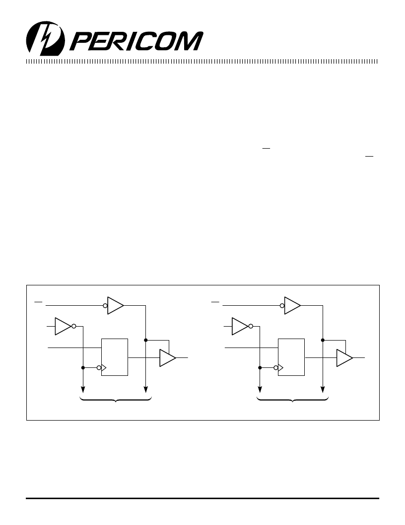
Logic Block Diagram
1
OE
1
CLK
1
O
0
C
D
1
D
0
TO 7 OTHER CHANNELS
2
OE
2
CLK
2
O
0
C
D
2
D
0
TO 7 OTHER CHANNELS
12345678901234567890123456789012123456789012345678901234567890121234567890123456789012345678901212345678901234567890123456789012123456789012
12345678901234567890123456789012123456789012345678901234567890121234567890123456789012345678901212345678901234567890123456789012123456789012
Fast CMOS 3.3V
16-Bit Register (3-State)
Product Features
Advanced Low Power CMOS Operation
Can serve as a 5V to 3V translator
Excellent output drive capability:
Balanced drives (24 mA sink and source)
Compatible with LVC
TM
class of products.
Pin compatible with industry standard
double-density pinouts
Low ground bounce outputs
Hysteresis on all inputs
Industrial operating temperature range: –40°C to +85°C
Inputs can be driven by 3.3V or 5V devices
Multiple center pin and distributed Vcc/GND pins
minimizing switching noise
Packages available:
– 48-pin 240 mil wide plastic TSSOP (A)
– 48-pin 300 mil wide plastic SSOP (V)
– 48-pin 173 mil wide plastic TVSOP (K)
Product Description
Pericom Semiconductor’s PI74FCT series of logic circuits are
produced in the Company’s advanced 0.6 micron CMOS tech-
nology, achieving industry leading speed grades.
The PI74FCT163374 is a 16-bit octal register designed with 16
D-type flip-flops with a buffered common clock and 3-state outputs.
The Output Enable (xOE) and clock (xCLK) controls are organized
to operate as two 8-bit registers or one 16-bit register. When OE is
HIGH, the outputs are in the high-impedance state. Input data
meeting the setup and hold time requirements of the D inputs is
transferred to the O outputs on the LOW-to-HIGH transition of the
clock input.
相關(guān)PDF資料 |
PDF描述 |
|---|---|
| PI74FCT2244ATH | Fast CMOS Octal Buffer/Line Drivers |
| PI74FCT244CTQ | Fast CMOS Octal Buffer/Line Drivers |
| PI74FCT244CTS | Fast CMOS Octal Buffer/Line Drivers |
| PI74FCT244DTQ | Fast CMOS Octal Buffer/Line Drivers |
| PI74FCT244DTS | Fast CMOS Octal Buffer/Line Drivers |
相關(guān)代理商/技術(shù)參數(shù) |
參數(shù)描述 |
|---|---|
| PI74FCT163374A | 制造商:未知廠家 制造商全稱:未知廠家 功能描述:16-Bit D-Type Flip-Flop |
| PI74FCT163374AA | 制造商:未知廠家 制造商全稱:未知廠家 功能描述:16-Bit D-Type Flip-Flop |
| PI74FCT163374AK | 制造商:未知廠家 制造商全稱:未知廠家 功能描述:16-Bit D-Type Flip-Flop |
| PI74FCT163374ATA | 制造商:未知廠家 制造商全稱:未知廠家 功能描述:16-Bit D-Type Flip-Flop |
| PI74FCT163374ATV | 制造商:未知廠家 制造商全稱:未知廠家 功能描述:16-Bit D-Type Flip-Flop |
發(fā)布緊急采購,3分鐘左右您將得到回復(fù)。