- 您現(xiàn)在的位置:買賣IC網(wǎng) > PDF目錄368010 > PI74FCT244T (Pericom Semiconductor Corp.) Fast CMOS Octal Buffer/Line Drivers PDF資料下載
參數(shù)資料
| 型號: | PI74FCT244T |
| 廠商: | Pericom Semiconductor Corp. |
| 英文描述: | Fast CMOS Octal Buffer/Line Drivers |
| 中文描述: | 快速CMOS八路緩沖器/線路驅(qū)動器 |
| 文件頁數(shù): | 3/7頁 |
| 文件大小: | 434K |
| 代理商: | PI74FCT244T |
3
PS2011D 09/22/04
PI74FCT244T/2244T
PI74FCT541T/2541T
Octal Buffer/Line Drivers
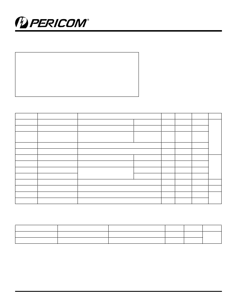
Maximum Ratings
(Above which the useful life may be impaired. For user guidelines, not tested.)
Note:
Stresses greater than those listed under MAXIMUM
RATINGS may cause permanent damage to the
device. This is a stress rating only and functional
operation of the device at these or any other con-
ditions above those indicated in the operational
sections of this specification is not implied. Exposure to
absolute maximum rating conditions for extended periods
may affect reliability.
DC Electrical Characteristics
(Over the Operating Range, TA = –40°C to +85°C, VCC = 5.0V ± 5%)
Parameters
Description
V
OH
Output HIGH Voltage
V
CC
= Min.,
V
IN
= V
IH
or
V
IL
V
OL
Output LOW Current
V
CC
= Min.,
V
IN
= V
IH
or
V
IL
Test Conditions
(1)
Min.
2.4
Typ
(2)
3.0
0.3
Max.
Units
I
OH
= –15.0mA
I
OL
= 64mA
I
OL
= 12mA
(25ΩSeries)
V
0.55
V
OL
Output LOW Current
V
CC
= Min.,
V
IN
= V
IH
or
V
IL
0.3
0.50
V
IH
V
IL
I
IH
I
IL
I
OZH
I
OZL
V
IK
I
OFF
I
OS
V
H
Input HIGH Voltage
Input LOW Voltage
Input HIGH Current
Input LOW Current
High Impedance
Output Current
Clamp Diode Voltage
Power Down Disable
Short Circuit Current
Input Hysteresis
Guaranteed Logic HIGH Level
Guaranteed Logic LOW Level
V
CC
=
Max.
V
CC
=
Max.
2.0
0.8
1
–1
1
–1
–1.2
100
V
IN
= V
CC
V
IN
= GND
V
OUT
= 2.7V
V
OUT
= 0.5V
μ
A
V
CC
= M
AX
.
V
CC
=
Min.,
I
IN
= –18
mA
V
CC
=
GND
, V
OUT
= 4.5V
V
CC
=
Max.
(3)
, V
OUT
= GND
–0.7
—
–120
200
V
μA
—
–60
mA
Capacitance
(
T
A
= 25°C, f = 1 MHz)
Parameters
(4)
C
IN
C
OUT
Description
Test Conditions
Typ.
Max.
Units
Input Capacitance
Output Capacitance
V
IN
= 0V
V
OUT
= 0V
6
8
10
12
pF
Notes:
1. For Max. or Min. conditions, use appropriate value specified under Electrical Characteristics for the applicable device type.
2. Typical values are at Vcc = 5.0V, +25°C ambient and maximum loading.
3. Not more than one output should be shorted at one time. Duration of the test should not exceed one second.
4. This parameter is determined by device characterization but is not production tested.
Storage Temperature.............................................................–65°C to +150°C
Ambient Temperature with Power Applied .............................-40°C to +85°C
Supply Voltage to Ground Potential (Inputs & Vcc Only) ......–0.5V to +7.0V
Supply Voltage to Ground Potential (Outputs & D/O Only)...–0.5V to +7.0V
DC Input Voltage .....................................................................–0.5V to +7.0V
DC Output Current................................................................................ 120mA
Power Dissipation.................................................................................... 0.5W
相關(guān)PDF資料 |
PDF描述 |
|---|---|
| PI74FCT244TH | Fast CMOS Octal Buffer/Line Drivers |
| PI74FCT244TL | Fast CMOS Octal Buffer/Line Drivers |
| PI74FCT244TLE | Fast CMOS Octal Buffer/Line Drivers |
| PI74FCT244TQ | Fast CMOS Octal Buffer/Line Drivers |
| PI74FCT244TS | Fast CMOS Octal Buffer/Line Drivers |
相關(guān)代理商/技術(shù)參數(shù) |
參數(shù)描述 |
|---|---|
| PI74FCT244TLE | 功能描述:緩沖器和線路驅(qū)動器 Octal Buffer Line Driver RoHS:否 制造商:Micrel 輸入線路數(shù)量:1 輸出線路數(shù)量:2 極性:Non-Inverting 電源電壓-最大:+/- 5.5 V 電源電壓-最小:+/- 2.37 V 最大工作溫度:+ 85 C 安裝風(fēng)格:SMD/SMT 封裝 / 箱體:MSOP-8 封裝:Reel |
| PI74FCT244TLEX | 功能描述:緩沖器和線路驅(qū)動器 Octal Buffer Line Driver RoHS:否 制造商:Micrel 輸入線路數(shù)量:1 輸出線路數(shù)量:2 極性:Non-Inverting 電源電壓-最大:+/- 5.5 V 電源電壓-最小:+/- 2.37 V 最大工作溫度:+ 85 C 安裝風(fēng)格:SMD/SMT 封裝 / 箱體:MSOP-8 封裝:Reel |
| PI74FCT244TQ | 制造商:Pericom Semiconductor Corporation 功能描述:Buffer/Line Driver 8-CH Non-Inverting 3-ST CMOS 20-Pin QSOP Tube 制造商:Pericom Semiconductor Corporation 功能描述:Driver/Buffer Device, Dual, 4-Bit, 20 Pin, Plastic, SSOP |
| PI74FCT244TQA | 制造商:. 功能描述: |
| PI74FCT244TQC | 制造商:Pericom Semiconductor Corporation 功能描述:ELECTRONIC COMPONENT |
發(fā)布緊急采購,3分鐘左右您將得到回復(fù)。