- 您現在的位置:買賣IC網 > PDF目錄370007 > PLSI1016E80LT44 (Lattice Semiconductor Corporation) High-Density Programmable Logic PDF資料下載
參數資料
| 型號: | PLSI1016E80LT44 |
| 廠商: | Lattice Semiconductor Corporation |
| 英文描述: | High-Density Programmable Logic |
| 中文描述: | 高密度可編程邏輯 |
| 文件頁數: | 4/15頁 |
| 文件大小: | 208K |
| 代理商: | PLSI1016E80LT44 |

4
1996 ISP Encyclopedia
Specifications
ispLSI and pLSI 1016E
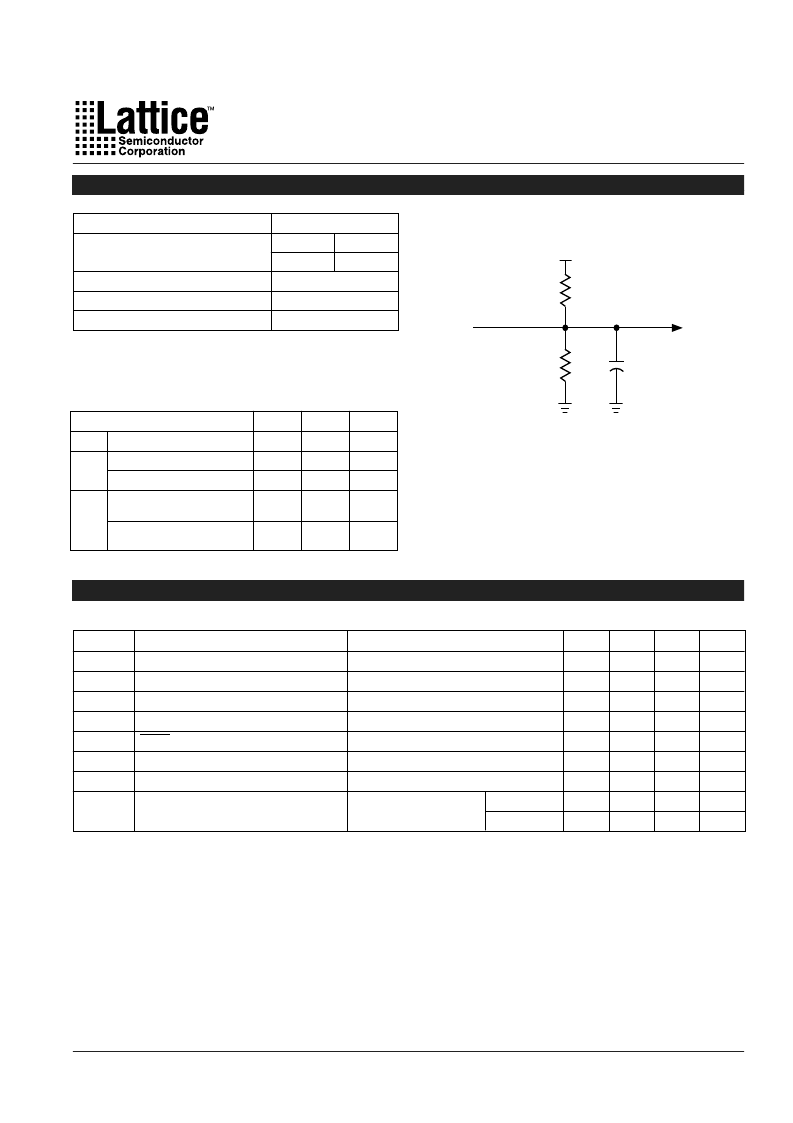
Switching Test Conditions
Figure 2. Test Load
DC Electrical Characteristics
Over Recommended Operating Conditions
Input Pulse Levels
Table 2-0003/1016E
Input Rise and Fall Time
10% to 90%
Input Timing Reference Levels
Ouput Timing Reference Levels
Output Load
GND to 3.0V
-125
-100, -80
1.5V
1.5V
See figure 2
3-state levels are measured 0.5V from
steady-state active level.
≤
2 ns
≤
3 ns
Output Load Conditions (see figure 2)
TEST CONDITION
R1
470
∞
470
R2
390
390
390
CL
35pF
35pF
35pF
A
B
Active High
Active Low
Active High to Z
at
V
OH
C
470
390
5pF
∞
390
5pF
Active Low to Z
at
V
OL
Table 2-0004/1016E
+ 5V
R1
R2
CL
*
Device
Output
Test
Point
*
CL includes Test Fixture and Probe Capacitance.
0213a
V
OL
V
OH
I
IL
SYMBOL
1. One output at a time for a maximum duration of one second. V = 0.5V was selected to avoid test problems
by tester ground degradation. Guaranteed but not 100% tested.
2. Measured using four 16-bit counters.
3. Typical values are at V = 5V and T = 25
°
C.
4. Maximum I varies widely with specific device configuration and operating frequency. Refer to the Power Consumption
section of this data sheet and Thermal Management section of the Lattice Semiconductor Data Book to estimate maximum
I .
Table 2-0007/1016E
1
I
IH
I
IL-isp
I
IL-PU
I
OS
PARAMETER
2, 4
I
CC
Output Low Voltage
Output High Voltage
Input or I/O Low Leakage Current
Input or I/O High Leakage Current
ispEN Input Low Leakage Current
I/O Active Pull-Up Current
Output Short Circuit Current
Operating Power Supply Current
I = 8 mA
I = -4 mA
0V
≤
V
≤
V (Max.)
IN
3.5V
≤
V
≤
V
0V
≤
V
≤
V
0V
≤
V
≤
V
V = 5V, V = 0.5V
V = 0.5V, V = 3.0V
f = 1 MHz
IN
CC
IN
IL
IN
IL
CONDITION
MIN.
–
2.4
–
TYP.
–
–
–
MAX.
0.4
–
-10
UNITS
V
V
μ
A
3
–
–
–
–
–
–
–
–
–
–
90
90
10
-150
-150
-200
–
–
μ
A
μ
A
μ
A
mA
mA
mA
Commercial
Industrial
相關PDF資料 |
PDF描述 |
|---|---|
| PLSI1016E80LT44I | High-Density Programmable Logic |
| PLSI1032-60LJ | High-Density Programmable Logic |
| PLSI1032-60LJI | KPSE06F14-15PF0 |
| PLSI1032-60LT | High-Density Programmable Logic |
| PLSI1032-80LJ | High-Density Programmable Logic |
相關代理商/技術參數 |
參數描述 |
|---|---|
| PLSI1016E80LT44I | 制造商:LATTICE 制造商全稱:Lattice Semiconductor 功能描述:High-Density Programmable Logic |
| PLSI1024-50LJ | 制造商:未知廠家 制造商全稱:未知廠家 功能描述:Electrically-Erasable Complex PLD |
| PLSI1024-60LH/883 | 制造商:未知廠家 制造商全稱:未知廠家 功能描述:Electrically-Erasable Complex PLD |
| PLSI1024-60LJ | 制造商:未知廠家 制造商全稱:未知廠家 功能描述:Electrically-Erasable Complex PLD |
| PLSI1024-60LJI | 制造商:未知廠家 制造商全稱:未知廠家 功能描述:Electrically-Erasable Complex PLD |
發(fā)布緊急采購,3分鐘左右您將得到回復。