- 您現(xiàn)在的位置:買賣IC網(wǎng) > PDF目錄378056 > PM7350-PI (PMC-SIERRA INC) DUAL SERIAL LINK PHY MULTIPLEXER PDF資料下載
參數(shù)資料
| 型號(hào): | PM7350-PI |
| 廠商: | PMC-SIERRA INC |
| 元件分類: | 數(shù)字傳輸電路 |
| 英文描述: | DUAL SERIAL LINK PHY MULTIPLEXER |
| 中文描述: | ATM/SONET/SDH SUPPORT CIRCUIT, PBGA160 |
| 封裝: | 15 X 15 MM, 1.81 MM HEIGHT, PLASTIC, BGA-160 |
| 文件頁數(shù): | 1/2頁 |
| 文件大?。?/td> | 35K |
| 代理商: | PM7350-PI |
PMC-990147 (P2)
PROPRIETARY AND CONFIDENTIAL TO PMC-SIERRA, INC. AND FOR ITS CUSTOMERS’ INTERNAL USE
1999 PMC-Sierra, Inc.
PMC-Sierra,Inc.
Dual Serial Link, PHY Multiplexer
PM7350
S/UNI-DUPLEX
FEATURES
Integrated analog/digital device that
interfaces a UTOPIA L2 bus to a serial
backplane with optional 1:1 protection
using high speed Low Voltage
Differential Signal (LVDS) serial links.
For framers or modems without
UTOPIA bus interfaces: optionally
provides cell delineation (I.432) across
16 clock and data (bit serial)
interfaces.
Interworks with PM7351
S/UNI-VORTEX devices to implement
a point-to-multipoint serial backplane
architecture, with optional 1:1
protection of the common card.
Interfaces to another S/UNI-DUPLEX
device (via a single LVDS link) to
create a simple point-to-point “UTOPIA
bus extension” capability.
Interfaces to two S/UNI-DUPLEX
devices to create a 1:1 protected bus
extension.
Requires no external memory devices.
Low power 3.3V CMOS technology.
Standard 5 pin P1149 JTAG port.
160 ball PBGA, 15mm x 15mm.
In the LVDS receive direction: selects
traffic from the LVDS link marked
active and demultiplexes the individual
cell streams to the appropriate PHY
device.
In the LVDS transmit direction: accepts
52-56 byte cell streams from up to 32
UTOPIA L2 compatible PHY devices,
multiplexing into a single cell stream
carried over two high speed LVDS
serial interfaces.
Cell read/write to both LVDS links
available through the processor port.
Provides optional hardware assisted
CRC32 calculation across cells to
support an embedded inter-processor
communication channel across the
LVDS links.
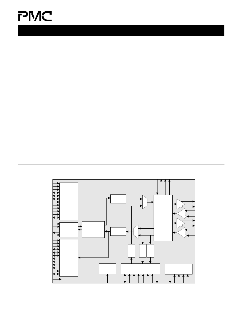
PHY/FRAMER INTERFACES
One of three modes can be selected:
8/16 bit, 33 MHz UTOPIA L2 bus
master (also supports expanded length
cells).
8/16 bit, 52 MHz extended UTOPIA L2
bus slave (compatible with PM7351
S/UNI-VORTEX).
16 port, 4 pin clocked serial data
interface (Tx & Rx), with integrated
I.432 ATM cell delineation.
LVDS INTERFACES
Dual 4 wire LVDS serial transceivers
each operating at up to 200 Mb/s.
Operates across PCB or backplane
traces, or across up to 10 meters of 4
wire twisted pair cabling for inter-shelf
communications.
Fully integrated LVDS clock synthesis
and recovery. No external analog
components are required.
Usable bandwidth (excludes system
overhead) of 186 Mb/s.
LVDS TRANSMIT DIRECTION
Simple round-robin multiplex of up to
32 PHYs (or 16 clock/data interfaces)
plus the microprocessor port’s cell
transfer buffer.
Multiplexed cell stream broadcast to
both LVDS simultaneously.
TXD1+
TXD1-
T
R
D
R
R
W
C
A
A
I
IENB
JTAG Test Access
Port
T
T
T
T
IADDR[4:0]
IAVALID
IDAT[15:0]
IPRTY
ISOC
ISX
IFCLK
ICA
SCI-PHY
Receive
Master/
Transmit
Slave
OENB
OADDR[4:0]
OAVALID
ODAT[15:0]
OPRTY
OSOC
OSX
OMASTER
OFCLK
OCA
SCI-PHY
Transmit
Master/
Receive Slave
T
Per-PHY
Buffers
2
B
4
F
RXD1+
RXD1-
Clock
Synthesis
R
R
R
TXD2+
TXD2-
RXD2+
RXD2-
4
F
Per-PHY
Buffers
IMASTER
IANYPHY
OANYPHY
SCIANY
LTXD[15:0]
LRXC[15:0]
LRXD[15:0]
Elastic Store
Cell Processor
IBUS8
OBUS8
Time-Sliced ATM
Transmission
Convergence
Microprocessor Interface
BLOCK DIAGRAM
相關(guān)PDF資料 |
PDF描述 |
|---|---|
| PM7351 | OCTAL SERIAL LINK MULTIPLEXER |
| PM7351-BI | OCTAL SERIAL LINK MULTIPLEXER |
| PM7364 | Frame Engine and Datalink Manager |
| PM7364-BI | FRAME ENGINE AND DATA LINK MANAGER |
| PM7366 | FRAME ENGINE AND DATA LINK MANAGER |
相關(guān)代理商/技術(shù)參數(shù) |
參數(shù)描述 |
|---|---|
| PM7351 | 制造商:PMC 制造商全稱:PMC 功能描述:Octal Serial Link Multiplexer |
| PM7351-BI | 制造商:PMC 制造商全稱:PMC 功能描述:OCTAL SERIAL LINK MULTIPLEXER |
| PM-736 | 制造商:Eclipse Tools 功能描述: |
| PM7364 | 制造商:PMC 制造商全稱:PMC 功能描述:FRAME ENGINE AND DATA LINK MANAGER |
| PM7364-BI | 制造商:PMC-Sierra 功能描述:PROTOCOL CONTROLLER, 256 Pin, BGA |
發(fā)布緊急采購,3分鐘左右您將得到回復(fù)。