- 您現(xiàn)在的位置:買賣IC網(wǎng) > PDF目錄69065 > PQ24050QGA20PKS-G (SYNQOR INC) 1-OUTPUT 100 W DC-DC REG PWR SUPPLY MODULE PDF資料下載
參數(shù)資料
| 型號(hào): | PQ24050QGA20PKS-G |
| 廠商: | SYNQOR INC |
| 元件分類: | 電源模塊 |
| 英文描述: | 1-OUTPUT 100 W DC-DC REG PWR SUPPLY MODULE |
| 封裝: | ROHS COMPLIANT PACKAGE-8 |
| 文件頁(yè)數(shù): | 6/13頁(yè) |
| 文件大小: | 540K |
| 代理商: | PQ24050QGA20PKS-G |
第1頁(yè)第2頁(yè)第3頁(yè)第4頁(yè)第5頁(yè)當(dāng)前第6頁(yè)第7頁(yè)第8頁(yè)第9頁(yè)第10頁(yè)第11頁(yè)第12頁(yè)第13頁(yè)
Product # PQ24050QGA20
Phone 1-888-567-9596
Doc.# 005-2QG250D Rev. C
03/13/06
Page 2
T
Technical S
echnical Specification
pecification
Input:
Output:
Current:
PPackage:
ackage:
18-36 V
5 V
20 A
Quarter-brick
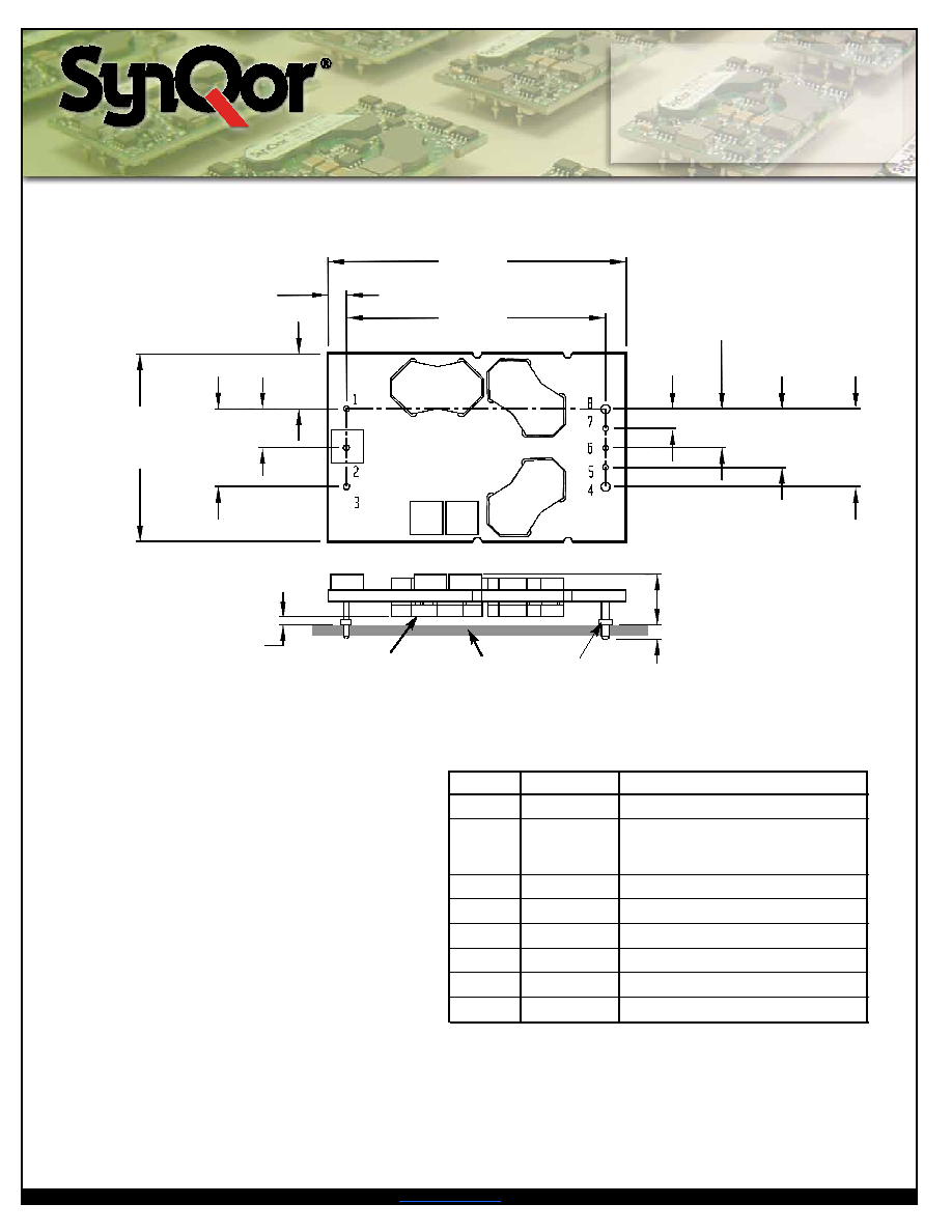
Pin No.
Name
Function
1
Vin(+)
Positive input voltage
2
ON/OFF
TTL input to turn converter
on and off, referenced to
Vin(-), with internal pull up.
3
Vin(-)
Negative input voltage
4
Vout(-)
Negative output voltage
5
SENSE(-)
Negative remote sense1
6
TRIM
Output voltage trim2
7
SENSE(+)
Positive remote sense3
8
Vout(+)
Positive output voltage
Notes:
1. SENSE(-) may be connected to Vout(-) or left open.
2. Leave TRIM pin open for nominal output voltage.
3. SENSE(+) may be connected to Vout(+) or left open.
NOTES
1) Pins 1-3, 5-7 are 0.040” (1.02mm) diameter with
0.080” (2.03 mm) diameter standoff shoulders.
2) Pins 4 and 8 are 0.062” (1.57 mm) diameter with
0.100” (2.54 mm) diameter standoff shoulders.
3) Other pin extension lengths available. Recommended pin
length is 0.03” (0.76mm) greater than the PCB thickness.
4) All Pins: Material - Copper Alloy
Finish - Tin/Lead over Nickel plate
5) Undimensioned components are shown for visual
reference only.
6) All dimensions in inches (mm)
Tolerances: x.xx +/-0.02 in. (x.x +/-0.5mm)
x.xxx +/-0.010 in. (x.xx +/-0.25mm)
7) Weight: 1.2 oz. (34 g) typical
8) Workmanship: Meets or exceeds IPC-A-610C Class II
9) UL/TUV standards require a clearance greater than 0.04”
(1.02mm) between input and output for Basic insulation. This
issue should be considered if any copper traces are on the top
side of the user’s board. Note that the ferrite cores are considered
part of the input/primary circuit.
10) The flanged pins are designed to permit surface mount sol-
dering (allowing to avoid the wave soldering process)
through the use of the flanged pin-in-paste technique.
0.300
(7.62)
0.600
(15.24)
1.45
(36.8)
0.43
(10.9)
0.150
(3.81)
0.300
(7.62)
0.450
(11.43)
0.600
(15.24)
0.14
(3.6)
2.30
(58.4)
2.00
(50.8)
Top View
Side View
PIN DESIGNATIONS
MECHANICAL
DIAGRAM
Load Board
Bottom side
Clearance
See Note 9
Max. Height
Lowest
Component
0.40
(10.2)
0.047+/-0.015
(1.19+/-0.38)
0.145
(3.68)
See Note 3
Flanged Pin
See Note 10
相關(guān)PDF資料 |
PDF描述 |
|---|---|
| PQ24050QGA20PNS | 1-OUTPUT 100 W DC-DC REG PWR SUPPLY MODULE |
| PQ24050QGA20PRS | 1-OUTPUT 100 W DC-DC REG PWR SUPPLY MODULE |
| PQ24120QGA08PNS | 1-OUTPUT 100 W DC-DC REG PWR SUPPLY MODULE |
| PQ24120QGA08NNS | 1-OUTPUT 100 W DC-DC REG PWR SUPPLY MODULE |
| PQ24120QGA08NYS | 1-OUTPUT 100 W DC-DC REG PWR SUPPLY MODULE |
相關(guān)代理商/技術(shù)參數(shù) |
參數(shù)描述 |
|---|---|
| PQ24050QGA20PNS | 制造商:SYNQOR 制造商全稱:SYNQOR 功能描述:Quarter-brick DC/DC Converter |
| PQ24050QGA20PRS | 制造商:SYNQOR 制造商全稱:SYNQOR 功能描述:Quarter-brick DC/DC Converter |
| PQ24050QGA20PYS | 制造商:SYNQOR 制造商全稱:SYNQOR 功能描述:Quarter-brick DC/DC Converter |
| PQ24120QEA25NRAG | 制造商:SynQor 功能描述:DC TO DC CONVERTER MODULE |
| PQ24120QGA08 | 制造商:SYNQOR 制造商全稱:SYNQOR 功能描述:100 Watts, No Heatsink, Isolated DC/DC Converter |
發(fā)布緊急采購(gòu),3分鐘左右您將得到回復(fù)。