- 您現(xiàn)在的位置:買賣IC網(wǎng) > PDF目錄69118 > PSC126-9IPD1 (POWER-ONE INC) 1-OUTPUT DC-DC REG PWR SUPPLY MODULE PDF資料下載
參數(shù)資料
| 型號(hào): | PSC126-9IPD1 |
| 廠商: | POWER-ONE INC |
| 元件分類: | 電源模塊 |
| 英文描述: | 1-OUTPUT DC-DC REG PWR SUPPLY MODULE |
| 文件頁(yè)數(shù): | 3/13頁(yè) |
| 文件大?。?/td> | 223K |
| 代理商: | PSC126-9IPD1 |
第1頁(yè)第2頁(yè)當(dāng)前第3頁(yè)第4頁(yè)第5頁(yè)第6頁(yè)第7頁(yè)第8頁(yè)第9頁(yè)第10頁(yè)第11頁(yè)第12頁(yè)第13頁(yè)

PSC Series Extended Data Sheet
Positive Switching Regulators (Rugged)
REV. MAY 12, 2004
Page 11 of 13
C
Crowbar
This option is recommended to protect the load against
power supply malfunction, but it is not designed to sink ex-
ternal currents.
A fixed-value monitoring circuit checks the output voltage
Vo. When the trigger voltage Vo c is reached, the thyristor
crowbar triggers and disables the output. It may be deacti-
vated by removal of the input voltage. In case of a switching
transistor defect, an internal fuse prevents excessive cur-
rent.
Note: As a central overvoltage protection device, the
crowbar is usually connected to the external load via
distributed inductance of the lines. For this reason, the
overvoltage at the load can temporarily exceed the trig-
ger voltage
Voc. Depending on the application, further
decentralized overvoltage protection elements may
have to be used additionally. For further information see:
Technical Information: Application Notes.
Description of Options
-9
Extended Temperature Range
The operational ambient temperature range is extended to
TA = –40 to 71°C. (TC = –40 to 95°C, TS = –55 to 100°C.)
P
Potentiometer
Option P excludes R function. The output voltage
Vo can be
adjusted with a screwdriver in the range from 0.92 - 1.08 of
the nominal output voltage
Vo nom.
However, the minimum differential voltage
DVio min between
input and output voltages as specified in:
Electrical Input
Data should be maintained.
L
Input Filter
Option L is recommended to reduce superimposed inter-
ference voltages and to prevent oscillations, if input lines
exceed approx. 5 m in total length. The fundamental wave
(approx. 120 kHz) of the reduced interference voltage be-
tween Vi+ and Gi– has, with an input line inductance of
5 H, a maximum magnitude of 4 mV AC.
The input impedance of the switching regulator at 120 kHz
is about 3.5
.The harmonics are small in comparison with
the fundamental wave. See also:
Electrical Input Data: RFI.
With option L, the maximum permissible additionally su-
perimposed ripple
ui of the input voltage (rectifier mode) at
a specified input frequency
fi has the following values:
ui max = 10 Vpp at 100 Hz or Vpp = 1000 Hz/fi 1V
D
Save Data Input Undervoltage Monitor
Note: Output instead of input undervoltage monitor is
available on request (Option D1).
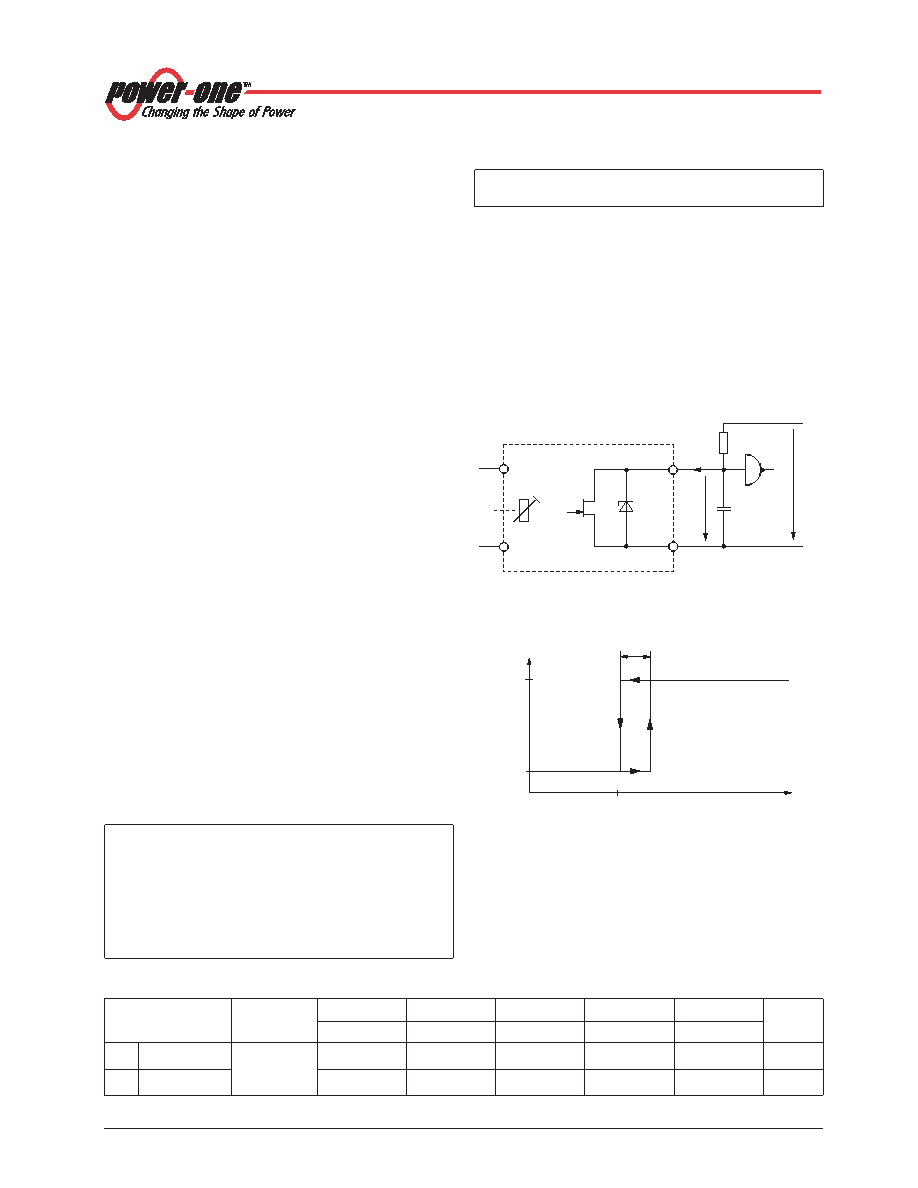
Terminal D and Go– are connected to a normally conduct-
ing field effect transistor (JFET). The switching characteris-
tics of the option D output are shown in fig. Definition of
Vt
and
VH. A 0.5 W Zener diode provides protection against
overvoltages.
The voltage
Vt can be externally adjusted with a trim poten-
tiometer by means of a screwdriver. The hysteresis
VH of Vt
is <2%. Terminal D stays low for a minimum time
tlow min, in
order to prevent any oscillation.
Vt can be set to a value
between
Vi min and Vi max. Please note that the JFET be-
comes conductive when
VD increases above 7 V approx.
Table 10: Crowbar trigger levels
Characteristics
Conditions
12 V
15 V
24 V
36 V
48 V
Unit
min
max
min
max
min
max
min
max
min
max
Vo c
Trigger voltage
Vi min - Vi max
13.5
16
16.5
19
27
31
40
45.5
55
60
V
Io = 0 - Io nom
t s
Delay time
TC min - TC max
1.5
s
Fig. 13
Test circuit with definition of voltage VD and current ID
Vi +
Gi –
Go –
8.2 V
D
VD
+5 V
100 pF
ID
10 k
JFET
Vt
11025
Fig. 14
Definition of Vt and VH
VD
VD high
VD low
Vt
Vi
VH
11026
相關(guān)PDF資料 |
PDF描述 |
|---|---|
| PSC156-7LIR | 1-OUTPUT DC-DC REG PWR SUPPLY MODULE |
| PSC156-9IPD1 | 1-OUTPUT DC-DC REG PWR SUPPLY MODULE |
| PSC156-7LIPCD | 1-OUTPUT DC-DC REG PWR SUPPLY MODULE |
| PSC366-9IPD1 | 1-OUTPUT DC-DC REG PWR SUPPLY MODULE |
| PSC246-7LIP | 1-OUTPUT DC-DC REG PWR SUPPLY MODULE |
相關(guān)代理商/技術(shù)參數(shù) |
參數(shù)描述 |
|---|---|
| PSC126-9IR | 制造商:Power-One 功能描述:DC/DC PS SGL-OUT 12V 6A 72W 9PIN - Bulk |
| PSC-12800A | 功能描述:電池充電器 12V 4-12AH 800mA AUTO. RoHS:否 制造商:Power-Sonic 化學(xué)性質(zhì):Sealed Lead Acid 輸出電壓:12 V 輸出電流:500 mA 端接類型:Screw |
| PSC-12800A-C | 功能描述:電池充電器 12V 4-8AH 800mA SWITCH-MODE CHARGER RoHS:否 制造商:Power-Sonic 化學(xué)性質(zhì):Sealed Lead Acid 輸出電壓:12 V 輸出電流:500 mA 端接類型:Screw |
| PSC128-7IR | 功能描述:SWITCHING REGULATOR 96W 12V RoHS:是 類別:電源 - 板載 >> DC DC Converters 系列:* 標(biāo)準(zhǔn)包裝:5 系列:* |
| PSC128-9IR | 制造商:Power-One 功能描述:DC/DC PS SGL-OUT 12V 8A 96W 9PIN - Bulk |
發(fā)布緊急采購(gòu),3分鐘左右您將得到回復(fù)。