- 您現(xiàn)在的位置:買賣IC網(wǎng) > PDF目錄376250 > PSD302-70JM (意法半導(dǎo)體) Low Cost Field Programmable Microcontroller Peripherals PDF資料下載
參數(shù)資料
| 型號(hào): | PSD302-70JM |
| 廠商: | 意法半導(dǎo)體 |
| 英文描述: | Low Cost Field Programmable Microcontroller Peripherals |
| 中文描述: | 低成本現(xiàn)場(chǎng)可編程微控制器外圍設(shè)備 |
| 文件頁數(shù): | 36/85頁 |
| 文件大小: | 691K |
| 代理商: | PSD302-70JM |
第1頁第2頁第3頁第4頁第5頁第6頁第7頁第8頁第9頁第10頁第11頁第12頁第13頁第14頁第15頁第16頁第17頁第18頁第19頁第20頁第21頁第22頁第23頁第24頁第25頁第26頁第27頁第28頁第29頁第30頁第31頁第32頁第33頁第34頁第35頁當(dāng)前第36頁第37頁第38頁第39頁第40頁第41頁第42頁第43頁第44頁第45頁第46頁第47頁第48頁第49頁第50頁第51頁第52頁第53頁第54頁第55頁第56頁第57頁第58頁第59頁第60頁第61頁第62頁第63頁第64頁第65頁第66頁第67頁第68頁第69頁第70頁第71頁第72頁第73頁第74頁第75頁第76頁第77頁第78頁第79頁第80頁第81頁第82頁第83頁第84頁第85頁

PSD3XX Famly
33
All the inputs shown, except CSI, go to the PAD logic. These signals must be taken into
consideration when calculating the composite frequency. Before we make the calculation,
let’s establish the following conditions:
The input with the highest frequency is ALE, which is 2 MHz. So our base period is
500 nsec for this example.
Only the address information from the multiplexed signals AD0-AD7 reach the PAD
logic because of the internal address latch. Signal transitions from data on AD0-AD7
do not reach the PADs.
The three inputs (Int, Sel, or Rdy) change state very infrequently relative to the 80C31
bus signals.
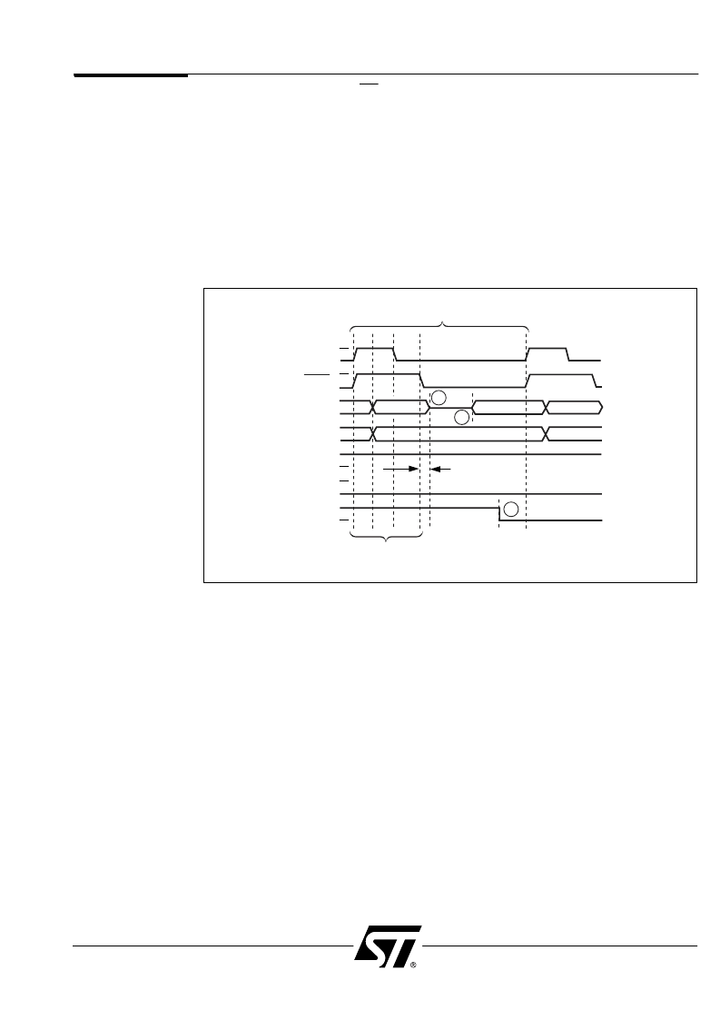
Now, lets assume the following is a snapshot in time of all the input signals during a typical
80C31 bus cycle. We’ll use a code fetch as an example since that happens most often.
16.0
Power
Management
(cont.)
ONE TYPICAL 80C31 BUS CYCLE (2 MHz, 500 nsec)
ALE
PSEN
AD0-AD7
A8-A15
INT
SEL
RDY
FOUR DISTINCT
TRANSITIONS
<25 nsec
ADDR
DATA
1
2
3
The calculation of the composite frequency is as follows:
There are four distinct transitions (first four dotted lines) within the base period of
500 nsec. These first four transitions all count toward the final composite frequency.
The transition at (1) in the diagram does not count as a distinct transition because it is
within 25 nsec of a neighboring transition (use 50 nsec for a ZPSD3XXV device).
Transition (2) above does not add to the composite frequency because only the
internally latched address signals reach the PADs, the data signal transitions do not.
The transition at (3) just happens to appear in this snapshot, but its frequency is so
low that it is not a significant contributor to the overall composite frequency, and will
not be used.
Divide the 500 nsec base period by the four (distinct transitions), yielding 125 nsec.
1/125 nsec = 8 MHz.
Use 8 MHz as the composite frequency of PAD inputs when calculating current
consumption. (See the next section for a sample current calculation.)
16.6 Loading on I/Opins
A final consideration when calculating the current usage for the entire PSD device is the
loading on I/O pins. All specifications for PSD current consumption in this document
assume zero current flowing through PSD I/O pins (including ADIO). I/O current is dictated
by the individual design implementation, and must be calculated by the designer. Be aware
that I/O current is a function of loading on the pins and the frequency at which the signals
toggle.
相關(guān)PDF資料 |
PDF描述 |
|---|---|
| PSD302-90J | Low Cost Field Programmable Microcontroller Peripherals |
| PSD302-90JI | Low Cost Field Programmable Microcontroller Peripherals |
| PSD302-90JM | Low Cost Field Programmable Microcontroller Peripherals |
| PSD302-A-15J | Low Cost Field Programmable Microcontroller Peripherals |
| PSD302-A-15JI | Low Cost Field Programmable Microcontroller Peripherals |
相關(guān)代理商/技術(shù)參數(shù) |
參數(shù)描述 |
|---|---|
| PSD302-70LI | 制造商:未知廠家 制造商全稱:未知廠家 功能描述:Field-Programmable Peripheral |
| PSD302-70LM | 制造商:未知廠家 制造商全稱:未知廠家 功能描述:Field-Programmable Peripheral |
| PSD302-70Q | 制造商:未知廠家 制造商全稱:未知廠家 功能描述:Field-Programmable Peripheral |
| PSD302-70QI | 制造商:未知廠家 制造商全稱:未知廠家 功能描述:Field-Programmable Peripheral |
| PSD302-70U | 制造商:未知廠家 制造商全稱:未知廠家 功能描述:Field-Programmable Peripheral |
發(fā)布緊急采購,3分鐘左右您將得到回復(fù)。