- 您現(xiàn)在的位置:買賣IC網(wǎng) > PDF目錄376249 > PSD312-15J (意法半導(dǎo)體) Low Cost Field Programmable Microcontroller Peripherals PDF資料下載
參數(shù)資料
| 型號(hào): | PSD312-15J |
| 廠商: | 意法半導(dǎo)體 |
| 英文描述: | Low Cost Field Programmable Microcontroller Peripherals |
| 中文描述: | 低成本現(xiàn)場可編程微控制器外圍設(shè)備 |
| 文件頁數(shù): | 10/85頁 |
| 文件大小: | 691K |
| 代理商: | PSD312-15J |
第1頁第2頁第3頁第4頁第5頁第6頁第7頁第8頁第9頁當(dāng)前第10頁第11頁第12頁第13頁第14頁第15頁第16頁第17頁第18頁第19頁第20頁第21頁第22頁第23頁第24頁第25頁第26頁第27頁第28頁第29頁第30頁第31頁第32頁第33頁第34頁第35頁第36頁第37頁第38頁第39頁第40頁第41頁第42頁第43頁第44頁第45頁第46頁第47頁第48頁第49頁第50頁第51頁第52頁第53頁第54頁第55頁第56頁第57頁第58頁第59頁第60頁第61頁第62頁第63頁第64頁第65頁第66頁第67頁第68頁第69頁第70頁第71頁第72頁第73頁第74頁第75頁第76頁第77頁第78頁第79頁第80頁第81頁第82頁第83頁第84頁第85頁

PSD3XX Famly
7
7.0
ZPSD
Background
(cont.)
Integrated Power Management
TM
Operation
Upon each address or logic input change to the ZPSD, the device powers up from low
power standby for a short time. Then the ZPSD consumes only the necessary power to
deliver new logic or memory data to its outputs as a response to the input change. After the
new outputs are stable, the ZPSD latches them and automatically reverts back to standby
mode. The I
CC
current flowing during standby mode and during DC operation is identical
and is only a few microamperes.
The ZPSD automatically reduces its DC current drain to these low levels and does not
require controlling by the CSI (Chip Select Input). Disabling the CSI pin unconditionally
forces the ZPSD to standby mode independent of other input transitions.
The only significant power consumption in the ZPSD occurs during AC operation.
The ZPSD contains the first architecture to apply zero power techniques to memory and
logic blocks.
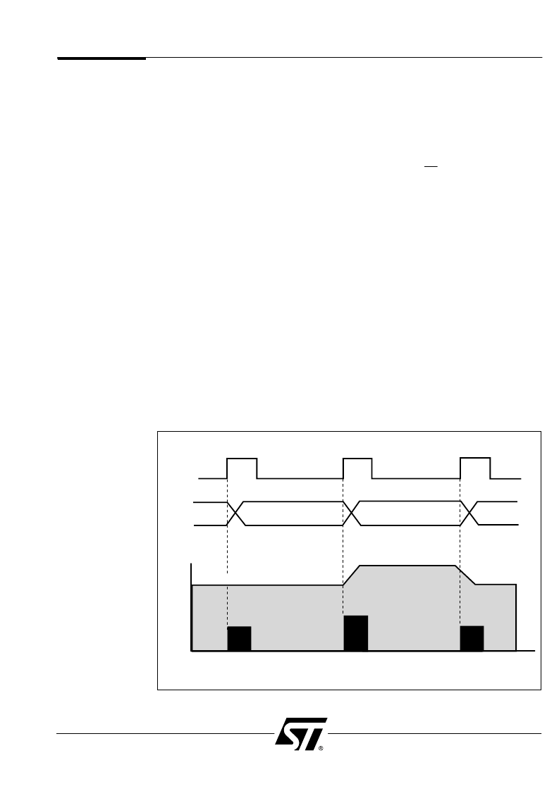
Figure 2 compares ZPSD zero power operation to the operation of a discrete solution.
A standard microcontroller (MCU) bus cycle usually starts with an ALE (or AS) pulse and
the generation of an address. The ZPSD detects the address transition and powers up for a
short time. The ZPSD then latches the outputs of the PAD, EPROM and SRAM to the new
values. After finishing these operations, the ZPSD shuts off its internal power, entering
standby mode. The time taken for the entire cycle is less than the ZPSD’s “access time.”
The ZPSD will stay in standby mode while its inputs are not changing between bus cycles.
In an alternate system implementation using discrete EPROM, SRAM, and other discrete
components, the system will consume operating power during the entire bus cycle. This
is because the chip select inputs on the memory devices are usually active throughout
the entire cycle. The AC power consumption of the ZPSD may be calculated using the
composite frequency of the MCU address and control signals, as well as any other logic
inputs to the ZPSD.
ALE
DISCRETE EPROM, SRAM & LOGIC
ADDRESS
EPROM
ACCESS
SRAM
ACCESS
EPROM
ACCESS
I
CC
ZPSD
ZPSD
ZPSD
TIME
Figure 2. ZPSDPower Operation vs. Dscrete Implementation
相關(guān)PDF資料 |
PDF描述 |
|---|---|
| PSD312-15JI | Low Cost Field Programmable Microcontroller Peripherals |
| PSD312-15JM | Low Cost Field Programmable Microcontroller Peripherals |
| PSD312R-15J | Low Cost Field Programmable Microcontroller Peripherals |
| PSD312R-15JI | Low Cost Field Programmable Microcontroller Peripherals |
| PSD312R-15JM | Low Cost Field Programmable Microcontroller Peripherals |
相關(guān)代理商/技術(shù)參數(shù) |
參數(shù)描述 |
|---|---|
| PSD312-15JI | 制造商:STMICROELECTRONICS 制造商全稱:STMicroelectronics 功能描述:Low Cost Field Programmable Microcontroller Peripherals |
| PSD312-15JM | 制造商:STMICROELECTRONICS 制造商全稱:STMicroelectronics 功能描述:Low Cost Field Programmable Microcontroller Peripherals |
| PSD312-15LI | 制造商:未知廠家 制造商全稱:未知廠家 功能描述:Field-Programmable Peripheral |
| PSD312-15LM | 制造商:未知廠家 制造商全稱:未知廠家 功能描述:Field-Programmable Peripheral |
| PSD312-15Q | 制造商:未知廠家 制造商全稱:未知廠家 功能描述:Field-Programmable Peripheral |
發(fā)布緊急采購,3分鐘左右您將得到回復(fù)。