- 您現(xiàn)在的位置:買賣IC網(wǎng) > PDF目錄368183 > PSD4235F3V-90JI (意法半導(dǎo)體) Flash In-System-Programmable Peripherals for 16-Bit MCUs PDF資料下載
參數(shù)資料
| 型號: | PSD4235F3V-90JI |
| 廠商: | 意法半導(dǎo)體 |
| 英文描述: | Flash In-System-Programmable Peripherals for 16-Bit MCUs |
| 中文描述: | Flash在系統(tǒng)可編程外設(shè)的16位微控制器 |
| 文件頁數(shù): | 56/93頁 |
| 文件大小: | 503K |
| 代理商: | PSD4235F3V-90JI |
第1頁第2頁第3頁第4頁第5頁第6頁第7頁第8頁第9頁第10頁第11頁第12頁第13頁第14頁第15頁第16頁第17頁第18頁第19頁第20頁第21頁第22頁第23頁第24頁第25頁第26頁第27頁第28頁第29頁第30頁第31頁第32頁第33頁第34頁第35頁第36頁第37頁第38頁第39頁第40頁第41頁第42頁第43頁第44頁第45頁第46頁第47頁第48頁第49頁第50頁第51頁第52頁第53頁第54頁第55頁當(dāng)前第56頁第57頁第58頁第59頁第60頁第61頁第62頁第63頁第64頁第65頁第66頁第67頁第68頁第69頁第70頁第71頁第72頁第73頁第74頁第75頁第76頁第77頁第78頁第79頁第80頁第81頁第82頁第83頁第84頁第85頁第86頁第87頁第88頁第89頁第90頁第91頁第92頁第93頁
Preliminary Information
PSD4000 Series
53
The
PSD4000
Functional
Blocks
(cont.)
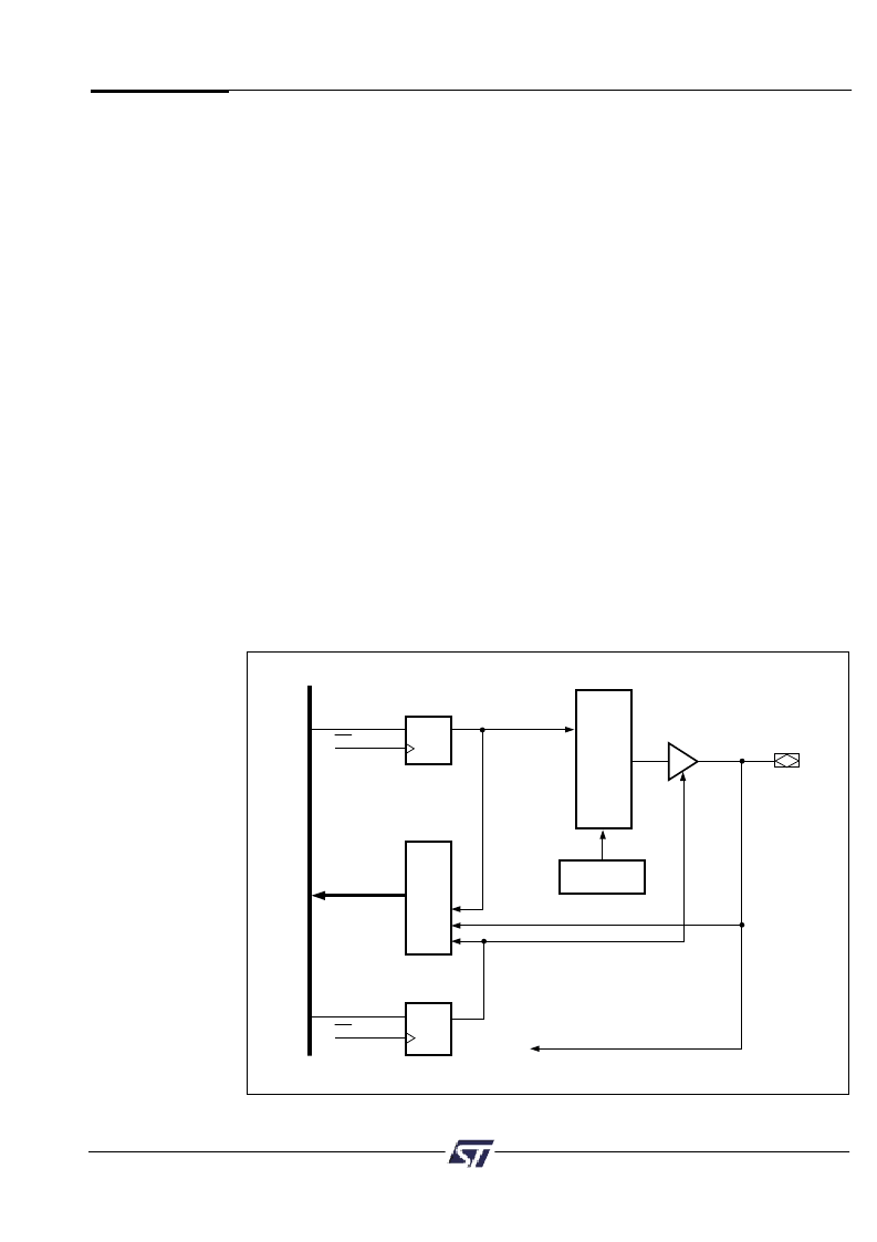
9.4.6 Port D – Functionality and Structure
Port D has four I/O pins. See Figure 22. Port D can be configured to program one or more
of the following functions:
J
MCU I/O Mode
J
PLD Input
–
direct input to PLD
Port D pins can be configured in PSDsoft as input pins for other dedicated functions:
J
PD0
–
ALE, as address strobe input
J
PD1
–
CLKIN, as clock input to the PLD and APD counter
J
PD2
–
CSI, as active low chip select input. A high input will disable the
Flash/SRAM and CSIOP.
J
PD3
–
WRH, as active low Write Enable (high byte) input or as DBE input from
68HC912
9.4.7 Port E – Functionality and Structure
Port E can be configured to perform one or more of the following functions (see Figure 23):
J
MCU I/O Mode
J
In-System Programming
–
JTAG port can be enabled for programming/erase of the
PSD4000 device. (See Section 9.6 for more information on JTAG programming.)
Pins that are configured as JTAG pins in PSDsoft will not be available for other I/O
functions.
J
Open Drain
–
Port E pins can be configured in Open Drain Mode
J
Battery Backup features
–
PE6 can be configured as a Battery Input (Vstby) pin.
PE7 can be configured as a Battery On Indicator output
pin, indicating when Vcc is less than Vbat.
J
Latched Address Output
–
Provided latched address (A7-0) output
I
DATA OUT
REG.
D
Q
D
Q
WR
WR
READ MUX
P
D
B
PLD INPUT
DIR REG.
DATA IN
OUTPUT
SELECT
OUTPUT
MUX
PORT D PIN
DATA OUT
Figure 22. Port D Structure
相關(guān)PDF資料 |
PDF描述 |
|---|---|
| PSD4235F3V-90M | Flash In-System-Programmable Peripherals for 16-Bit MCUs |
| PSD4235F3V-90MI | Flash In-System-Programmable Peripherals for 16-Bit MCUs |
| PSD4235F3V-90U | Flash In-System-Programmable Peripherals for 16-Bit MCUs |
| PSD4235F3V-90UI | Flash In-System-Programmable Peripherals for 16-Bit MCUs |
| PSD4235F3V-A-12B81I | Flash In-System-Programmable Peripherals for 16-Bit MCUs |
相關(guān)代理商/技術(shù)參數(shù) |
參數(shù)描述 |
|---|---|
| PSD4235G2-70U | 功能描述:SPLD - 簡單可編程邏輯器件 5.0V 4M 70ns RoHS:否 制造商:Texas Instruments 邏輯系列:TICPAL22V10Z 大電池?cái)?shù)量:10 最大工作頻率:66 MHz 延遲時(shí)間:25 ns 工作電源電壓:4.75 V to 5.25 V 電源電流:100 uA 最大工作溫度:+ 75 C 最小工作溫度:0 C 安裝風(fēng)格:Through Hole 封裝 / 箱體:DIP-24 |
| PSD4235G2-90U | 功能描述:CPLD - 復(fù)雜可編程邏輯器件 5.0V 4M 90ns RoHS:否 制造商:Lattice 系列: 存儲類型:EEPROM 大電池?cái)?shù)量:128 最大工作頻率:333 MHz 延遲時(shí)間:2.7 ns 可編程輸入/輸出端數(shù)量:64 工作電源電壓:3.3 V 最大工作溫度:+ 90 C 最小工作溫度:0 C 封裝 / 箱體:TQFP-100 |
| PSD4235G2-90UI | 功能描述:CPLD - 復(fù)雜可編程邏輯器件 5.0V 4M 90ns RoHS:否 制造商:Lattice 系列: 存儲類型:EEPROM 大電池?cái)?shù)量:128 最大工作頻率:333 MHz 延遲時(shí)間:2.7 ns 可編程輸入/輸出端數(shù)量:64 工作電源電壓:3.3 V 最大工作溫度:+ 90 C 最小工作溫度:0 C 封裝 / 箱體:TQFP-100 |
| PSD4235G2V-12UI | 功能描述:CPLD - 復(fù)雜可編程邏輯器件 3.3V 4M 120ns RoHS:否 制造商:Lattice 系列: 存儲類型:EEPROM 大電池?cái)?shù)量:128 最大工作頻率:333 MHz 延遲時(shí)間:2.7 ns 可編程輸入/輸出端數(shù)量:64 工作電源電壓:3.3 V 最大工作溫度:+ 90 C 最小工作溫度:0 C 封裝 / 箱體:TQFP-100 |
| PSD4235G2V-90U | 功能描述:CPLD - 復(fù)雜可編程邏輯器件 3.3V 4M 90ns RoHS:否 制造商:Lattice 系列: 存儲類型:EEPROM 大電池?cái)?shù)量:128 最大工作頻率:333 MHz 延遲時(shí)間:2.7 ns 可編程輸入/輸出端數(shù)量:64 工作電源電壓:3.3 V 最大工作溫度:+ 90 C 最小工作溫度:0 C 封裝 / 箱體:TQFP-100 |
發(fā)布緊急采購,3分鐘左右您將得到回復(fù)。