- 您現(xiàn)在的位置:買(mǎi)賣(mài)IC網(wǎng) > PDF目錄378071 > PSD813F4V-20 (意法半導(dǎo)體) Flash In-System Programmable (ISP) Peripherals for 8-bit MCUs, 5V PDF資料下載
參數(shù)資料
| 型號(hào): | PSD813F4V-20 |
| 廠商: | 意法半導(dǎo)體 |
| 英文描述: | Flash In-System Programmable (ISP) Peripherals for 8-bit MCUs, 5V |
| 中文描述: | Flash在系統(tǒng)可編程(ISP)的周邊8位MCU,5V的 |
| 文件頁(yè)數(shù): | 12/110頁(yè) |
| 文件大?。?/td> | 1685K |
| 代理商: | PSD813F4V-20 |
第1頁(yè)第2頁(yè)第3頁(yè)第4頁(yè)第5頁(yè)第6頁(yè)第7頁(yè)第8頁(yè)第9頁(yè)第10頁(yè)第11頁(yè)當(dāng)前第12頁(yè)第13頁(yè)第14頁(yè)第15頁(yè)第16頁(yè)第17頁(yè)第18頁(yè)第19頁(yè)第20頁(yè)第21頁(yè)第22頁(yè)第23頁(yè)第24頁(yè)第25頁(yè)第26頁(yè)第27頁(yè)第28頁(yè)第29頁(yè)第30頁(yè)第31頁(yè)第32頁(yè)第33頁(yè)第34頁(yè)第35頁(yè)第36頁(yè)第37頁(yè)第38頁(yè)第39頁(yè)第40頁(yè)第41頁(yè)第42頁(yè)第43頁(yè)第44頁(yè)第45頁(yè)第46頁(yè)第47頁(yè)第48頁(yè)第49頁(yè)第50頁(yè)第51頁(yè)第52頁(yè)第53頁(yè)第54頁(yè)第55頁(yè)第56頁(yè)第57頁(yè)第58頁(yè)第59頁(yè)第60頁(yè)第61頁(yè)第62頁(yè)第63頁(yè)第64頁(yè)第65頁(yè)第66頁(yè)第67頁(yè)第68頁(yè)第69頁(yè)第70頁(yè)第71頁(yè)第72頁(yè)第73頁(yè)第74頁(yè)第75頁(yè)第76頁(yè)第77頁(yè)第78頁(yè)第79頁(yè)第80頁(yè)第81頁(yè)第82頁(yè)第83頁(yè)第84頁(yè)第85頁(yè)第86頁(yè)第87頁(yè)第88頁(yè)第89頁(yè)第90頁(yè)第91頁(yè)第92頁(yè)第93頁(yè)第94頁(yè)第95頁(yè)第96頁(yè)第97頁(yè)第98頁(yè)第99頁(yè)第100頁(yè)第101頁(yè)第102頁(yè)第103頁(yè)第104頁(yè)第105頁(yè)第106頁(yè)第107頁(yè)第108頁(yè)第109頁(yè)第110頁(yè)
PSD813F1
12/110
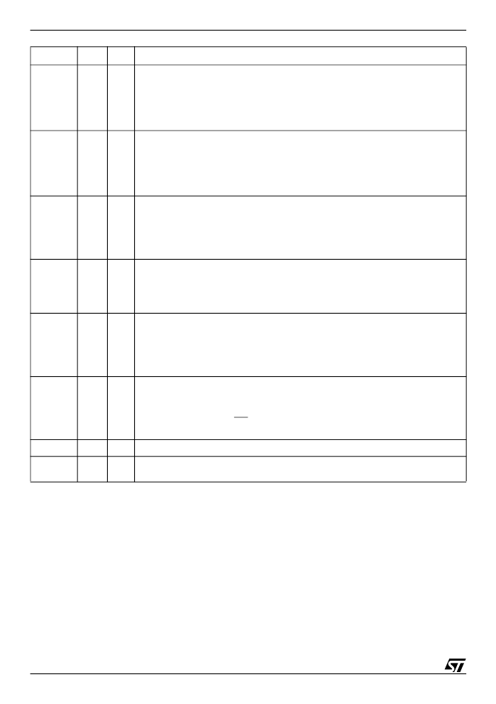
Note: 1. The pin numbers in this table are for the PLCC package only. See the
Figure 2., page 7
, for pin numbers on other package type.
2. These functions can be multiplexed with other functions.
PC5
13
I/O
PC5 pin of Port C. This port pin can be configured to have the following functions:
1. MCU I/O
–
write to or read from a standard output or input port.
2. CPLD macrocell (McellBC5) output.
3. Input to the PLDs.
4. TDI input
2
for the JTAG Interface.
This pin can be configured as a CMOS or Open Drain output.
PC6
12
I/O
PC6 pin of Port C. This port pin can be configured to have the following functions:
1. MCU I/O
–
write to or read from a standard output or input port.
2. CPLD macrocell (McellBC6) output.
3. Input to the PLDs.
4. TDO output
2
for the JTAG Interface.
This pin can be configured as a CMOS or Open Drain output.
PC7
11
I/O
PC7 pin of Port C. This port pin can be configured to have the following functions:
1. MCU I/O
–
write to or read from a standard output or input port.
2. CPLD macrocell (McellBC7) output.
3. Input to the PLDs.
4. DBE
–
active Low Data Byte Enable input from 68HC912 type MCUs.
This pin can be configured as a CMOS or Open Drain output.
PD0
10
I/O
PD0 pin of Port D. This port pin can be configured to have the following functions:
1. ALE/AS input latches address output from the MCU.
2. MCU I/O
–
write or read from a standard output or input port.
3. Input to the PLDs.
4. CPLD output (External Chip Select).
PD1
9
I/O
PD1 pin of Port D. This port pin can be configured to have the following functions:
1. MCU I/O
–
write to or read from a standard output or input port.
2. Input to the PLDs.
3. CPLD output (External Chip Select).
4. CLKIN
–
clock input to the CPLD macrocells, the APD Unit
’
s Power-down counter, and
the CPLD AND Array.
PD2
8
I/O
PD2 pin of Port D. This port pin can be configured to have the following functions:
1. MCU I/O
–
write to or read from a standard output or input port.
2. Input to the PLDs.
3. CPLD output (External Chip Select).
4. PSD Chip Select Input (CSI). When Low, the MCU can access the PSD memory and I/
O. When High, the PSD memory blocks are disabled to conserve power.
V
CC
15, 38
Supply Voltage
GND
1, 16,
26
Ground pins
Pin Name
Pin
Type
Description
(1)
相關(guān)PDF資料 |
PDF描述 |
|---|---|
| PSD813F4V-70 | Flash In-System Programmable (ISP) Peripherals for 8-bit MCUs, 5V |
| PSD813F4V-90 | Flash In-System Programmable (ISP) Peripherals for 8-bit MCUs, 5V |
| PSD813F5-12 | Flash In-System Programmable (ISP) Peripherals for 8-bit MCUs, 5V |
| PSD813F5-15 | Flash In-System Programmable (ISP) Peripherals for 8-bit MCUs, 5V |
| PSD813F5-20 | Flash In-System Programmable (ISP) Peripherals for 8-bit MCUs, 5V |
相關(guān)代理商/技術(shù)參數(shù) |
參數(shù)描述 |
|---|---|
| PSD813F4VA-15J | 功能描述:SPLD - 簡(jiǎn)單可編程邏輯器件 U 511-PSD813F2VA-15J RoHS:否 制造商:Texas Instruments 邏輯系列:TICPAL22V10Z 大電池?cái)?shù)量:10 最大工作頻率:66 MHz 延遲時(shí)間:25 ns 工作電源電壓:4.75 V to 5.25 V 電源電流:100 uA 最大工作溫度:+ 75 C 最小工作溫度:0 C 安裝風(fēng)格:Through Hole 封裝 / 箱體:DIP-24 |
| PSD813F4VA-15U | 功能描述:SPLD - 簡(jiǎn)單可編程邏輯器件 U 511-PSD813F2VA-15U RoHS:否 制造商:Texas Instruments 邏輯系列:TICPAL22V10Z 大電池?cái)?shù)量:10 最大工作頻率:66 MHz 延遲時(shí)間:25 ns 工作電源電壓:4.75 V to 5.25 V 電源電流:100 uA 最大工作溫度:+ 75 C 最小工作溫度:0 C 安裝風(fēng)格:Through Hole 封裝 / 箱體:DIP-24 |
| PSD813F5-12JI | 制造商:WSI 功能描述: |
| PSD813F5-15JI | 制造商:WSI 功能描述: |
| PSD813F5-15U | 制造商:WSI 功能描述: 制造商:WSI 功能描述:1M X 1 FLASH, 27 I/O, PIA-GENERAL PURPOSE, PQFP64 |
發(fā)布緊急采購(gòu),3分鐘左右您將得到回復(fù)。