- 您現(xiàn)在的位置:買賣IC網(wǎng) > PDF目錄368260 > PSD835G1V-B-20U (意法半導體) Configurable Memory System on a Chip for 8-Bit Microcontrollers PDF資料下載
參數(shù)資料
| 型號: | PSD835G1V-B-20U |
| 廠商: | 意法半導體 |
| 英文描述: | Configurable Memory System on a Chip for 8-Bit Microcontrollers |
| 中文描述: | 在8片位微控制器可配置存儲系統(tǒng) |
| 文件頁數(shù): | 32/110頁 |
| 文件大?。?/td> | 570K |
| 代理商: | PSD835G1V-B-20U |
第1頁第2頁第3頁第4頁第5頁第6頁第7頁第8頁第9頁第10頁第11頁第12頁第13頁第14頁第15頁第16頁第17頁第18頁第19頁第20頁第21頁第22頁第23頁第24頁第25頁第26頁第27頁第28頁第29頁第30頁第31頁當前第32頁第33頁第34頁第35頁第36頁第37頁第38頁第39頁第40頁第41頁第42頁第43頁第44頁第45頁第46頁第47頁第48頁第49頁第50頁第51頁第52頁第53頁第54頁第55頁第56頁第57頁第58頁第59頁第60頁第61頁第62頁第63頁第64頁第65頁第66頁第67頁第68頁第69頁第70頁第71頁第72頁第73頁第74頁第75頁第76頁第77頁第78頁第79頁第80頁第81頁第82頁第83頁第84頁第85頁第86頁第87頁第88頁第89頁第90頁第91頁第92頁第93頁第94頁第95頁第96頁第97頁第98頁第99頁第100頁第101頁第102頁第103頁第104頁第105頁第106頁第107頁第108頁第109頁第110頁
PSD835G2
PSD8XX Family
31
RESET
D0 - D7
R/W
D0
Q0
Q1
Q2
Q3
Q4
Q5
Q6
Q7
D1
D2
D3
D4
D5
D6
D7
PAGE
REGISTER
PGR0
PGR1
PGR2
PGR3
DPLD
AND
GPLD
INTERNAL
SELECTS
AND LOGIC
FLASH
PLD
PGR4
PGR5
PGR6
PGR7
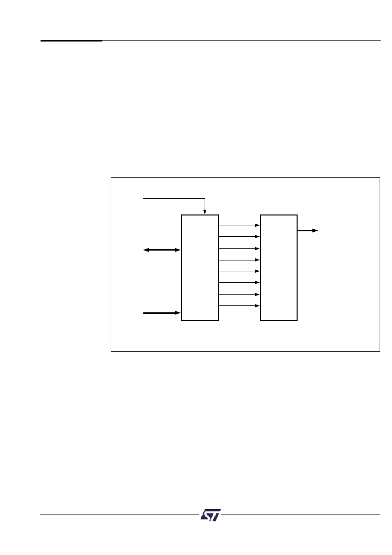
Figure 9. Page Register
The
PSD835G2
Functional
Blocks
(cont.)
9.1.4 Page Register
The eight bit Page Register increases the addressing capability of the microcontroller by a
factor of up to 256. The contents of the register can also be read by the microcontroller.
The outputs of the Page Register (PGR0-PGR7) are inputs to the PLD decoder and
can be included in the Flash Memory, secondary Flash memory, and SRAM chip select
equations.
If memory paging is not needed, or if not all 8 page register bits are needed for memory
paging, then these bits may be used in the PLD for general logic. See Application
Notes.
Figure 9 shows the Page Register. The eight flip flops in the register are connected to the
internal data bus D0-D7. The microcontroller can write to or read from the Page Register.
The Page Register can be accessed at address location CSIOP + E0h.
發(fā)布緊急采購,3分鐘左右您將得到回復。