- 您現(xiàn)在的位置:買賣IC網(wǎng) > PDF目錄368268 > PSD935F2-20MI (意法半導(dǎo)體) Configurable Memory System on a Chip for 8-Bit Microcontrollers PDF資料下載
參數(shù)資料
| 型號: | PSD935F2-20MI |
| 廠商: | 意法半導(dǎo)體 |
| 英文描述: | Configurable Memory System on a Chip for 8-Bit Microcontrollers |
| 中文描述: | 在8片位微控制器可配置存儲系統(tǒng) |
| 文件頁數(shù): | 41/91頁 |
| 文件大小: | 488K |
| 代理商: | PSD935F2-20MI |
第1頁第2頁第3頁第4頁第5頁第6頁第7頁第8頁第9頁第10頁第11頁第12頁第13頁第14頁第15頁第16頁第17頁第18頁第19頁第20頁第21頁第22頁第23頁第24頁第25頁第26頁第27頁第28頁第29頁第30頁第31頁第32頁第33頁第34頁第35頁第36頁第37頁第38頁第39頁第40頁當(dāng)前第41頁第42頁第43頁第44頁第45頁第46頁第47頁第48頁第49頁第50頁第51頁第52頁第53頁第54頁第55頁第56頁第57頁第58頁第59頁第60頁第61頁第62頁第63頁第64頁第65頁第66頁第67頁第68頁第69頁第70頁第71頁第72頁第73頁第74頁第75頁第76頁第77頁第78頁第79頁第80頁第81頁第82頁第83頁第84頁第85頁第86頁第87頁第88頁第89頁第90頁第91頁
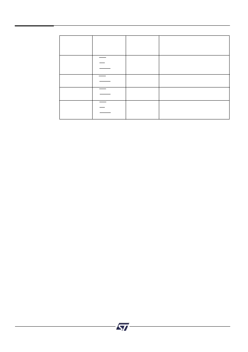
PSD9XX Family
PSD935G2
40
The
PSD935G2
Functional
Blocks
(cont.)
Configuration
80C251
Read/Write
Pins
Connecting to
PSD935G2
Pins
Page Mode
WR
RD
PSEN
CNTL0
CNTL1
CNTL2
Non-Page Mode, 80C31 compatible
A
[
7:0
]
multiplex with D
[
7:0
}
1
2
WR
PSEN only
CNTL0
CNTL1
Non-Page Mode
A
[
7:0
]
multiplex with D
[
7:0
}
3
WR
PSEN only
CNTL0
CNTL1
Page Mode
A
[
15:8
]
multiplex with D
[
7:0
}
4
WR
RD
PSEN
CNTL0
CNTL1
CNTL2
Page Mode
A
[
15:8
]
multiplex with D
[
7:0
}
Table 15. 80C251 Configurations
9.3.3.3 80C51XA
The Philips 80C51XA microcontroller family supports an 8- or 16-bit multiplexed bus that
can have burst cycles. Address bits A[3:0] are not multiplexed, while A[19:4] are
multiplexed with data bits D[15:0] in 16-bit mode. In 8-bit mode, A[11:4] are multiplexed
with data bits D[7:0].
The 80C51XA can be configured to operate in eight-bit data mode. (shown in Figure 18).
The 80C51XA improves bus throughput and performance by executing Burst cycles for
code fetches. In Burst Mode, address A19-4 are latched internally by the PSD935G2, while
the 80C51XA changes the A3-0 lines to fetch up to 16 bytes of code. The PSD access
time is then measured from address A3-A0 valid to data in valid. The PSD bus timing
requirement in Burst Mode is identical to the normal bus cycle, except the address setup
and hold time with respect to ALE does not apply.
9.3.3.4 68HC11
Figure 19 shows an interface to a 68HC11 where the PSD935G2 is configured in 8-bit
multiplexed mode with E and R/W settings. The DPLD can generate the READ and WR
signals for external devices.
相關(guān)PDF資料 |
PDF描述 |
|---|---|
| PSD935F2-20U | Configurable Memory System on a Chip for 8-Bit Microcontrollers |
| PSD935F2-20UI | Configurable Memory System on a Chip for 8-Bit Microcontrollers |
| PSD935F2-70B81 | Configurable Memory System on a Chip for 8-Bit Microcontrollers |
| PSD935F2-70B81I | Configurable Memory System on a Chip for 8-Bit Microcontrollers |
| PSD935F2-70J | Configurable Memory System on a Chip for 8-Bit Microcontrollers |
相關(guān)代理商/技術(shù)參數(shù) |
參數(shù)描述 |
|---|---|
| PSD935G2-90U | 功能描述:SPLD - 簡單可編程邏輯器件 TQFP-80 5V 4M 90N RoHS:否 制造商:Texas Instruments 邏輯系列:TICPAL22V10Z 大電池數(shù)量:10 最大工作頻率:66 MHz 延遲時間:25 ns 工作電源電壓:4.75 V to 5.25 V 電源電流:100 uA 最大工作溫度:+ 75 C 最小工作溫度:0 C 安裝風(fēng)格:Through Hole 封裝 / 箱體:DIP-24 |
| PSD935G2V-90U | 功能描述:SPLD - 簡單可編程邏輯器件 U 511-PSD835G2V-90U RoHS:否 制造商:Texas Instruments 邏輯系列:TICPAL22V10Z 大電池數(shù)量:10 最大工作頻率:66 MHz 延遲時間:25 ns 工作電源電壓:4.75 V to 5.25 V 電源電流:100 uA 最大工作溫度:+ 75 C 最小工作溫度:0 C 安裝風(fēng)格:Through Hole 封裝 / 箱體:DIP-24 |
| PSD954F2-90J | 功能描述:SPLD - 簡單可編程邏輯器件 U 511-PSD854F2-90J RoHS:否 制造商:Texas Instruments 邏輯系列:TICPAL22V10Z 大電池數(shù)量:10 最大工作頻率:66 MHz 延遲時間:25 ns 工作電源電壓:4.75 V to 5.25 V 電源電流:100 uA 最大工作溫度:+ 75 C 最小工作溫度:0 C 安裝風(fēng)格:Through Hole 封裝 / 箱體:DIP-24 |
| PSD954F2-90M | 功能描述:SPLD - 簡單可編程邏輯器件 U 511-PSD854F2-90M RoHS:否 制造商:Texas Instruments 邏輯系列:TICPAL22V10Z 大電池數(shù)量:10 最大工作頻率:66 MHz 延遲時間:25 ns 工作電源電壓:4.75 V to 5.25 V 電源電流:100 uA 最大工作溫度:+ 75 C 最小工作溫度:0 C 安裝風(fēng)格:Through Hole 封裝 / 箱體:DIP-24 |
| PSD954F2V-90J | 功能描述:SPLD - 簡單可編程邏輯器件 5.0V 2M 90ns RoHS:否 制造商:Texas Instruments 邏輯系列:TICPAL22V10Z 大電池數(shù)量:10 最大工作頻率:66 MHz 延遲時間:25 ns 工作電源電壓:4.75 V to 5.25 V 電源電流:100 uA 最大工作溫度:+ 75 C 最小工作溫度:0 C 安裝風(fēng)格:Through Hole 封裝 / 箱體:DIP-24 |
發(fā)布緊急采購,3分鐘左右您將得到回復(fù)。