- 您現(xiàn)在的位置:買賣IC網(wǎng) > PDF目錄368277 > PSD935G1V-A-70B81I (意法半導(dǎo)體) Configurable Memory System on a Chip for 8-Bit Microcontrollers PDF資料下載
參數(shù)資料
| 型號: | PSD935G1V-A-70B81I |
| 廠商: | 意法半導(dǎo)體 |
| 英文描述: | Configurable Memory System on a Chip for 8-Bit Microcontrollers |
| 中文描述: | 在8片位微控制器可配置存儲系統(tǒng) |
| 文件頁數(shù): | 29/91頁 |
| 文件大小: | 488K |
| 代理商: | PSD935G1V-A-70B81I |
第1頁第2頁第3頁第4頁第5頁第6頁第7頁第8頁第9頁第10頁第11頁第12頁第13頁第14頁第15頁第16頁第17頁第18頁第19頁第20頁第21頁第22頁第23頁第24頁第25頁第26頁第27頁第28頁當(dāng)前第29頁第30頁第31頁第32頁第33頁第34頁第35頁第36頁第37頁第38頁第39頁第40頁第41頁第42頁第43頁第44頁第45頁第46頁第47頁第48頁第49頁第50頁第51頁第52頁第53頁第54頁第55頁第56頁第57頁第58頁第59頁第60頁第61頁第62頁第63頁第64頁第65頁第66頁第67頁第68頁第69頁第70頁第71頁第72頁第73頁第74頁第75頁第76頁第77頁第78頁第79頁第80頁第81頁第82頁第83頁第84頁第85頁第86頁第87頁第88頁第89頁第90頁第91頁
PSD9XX Family
PSD935G2
28
The
PSD935G2
Functional
Blocks
(cont.)
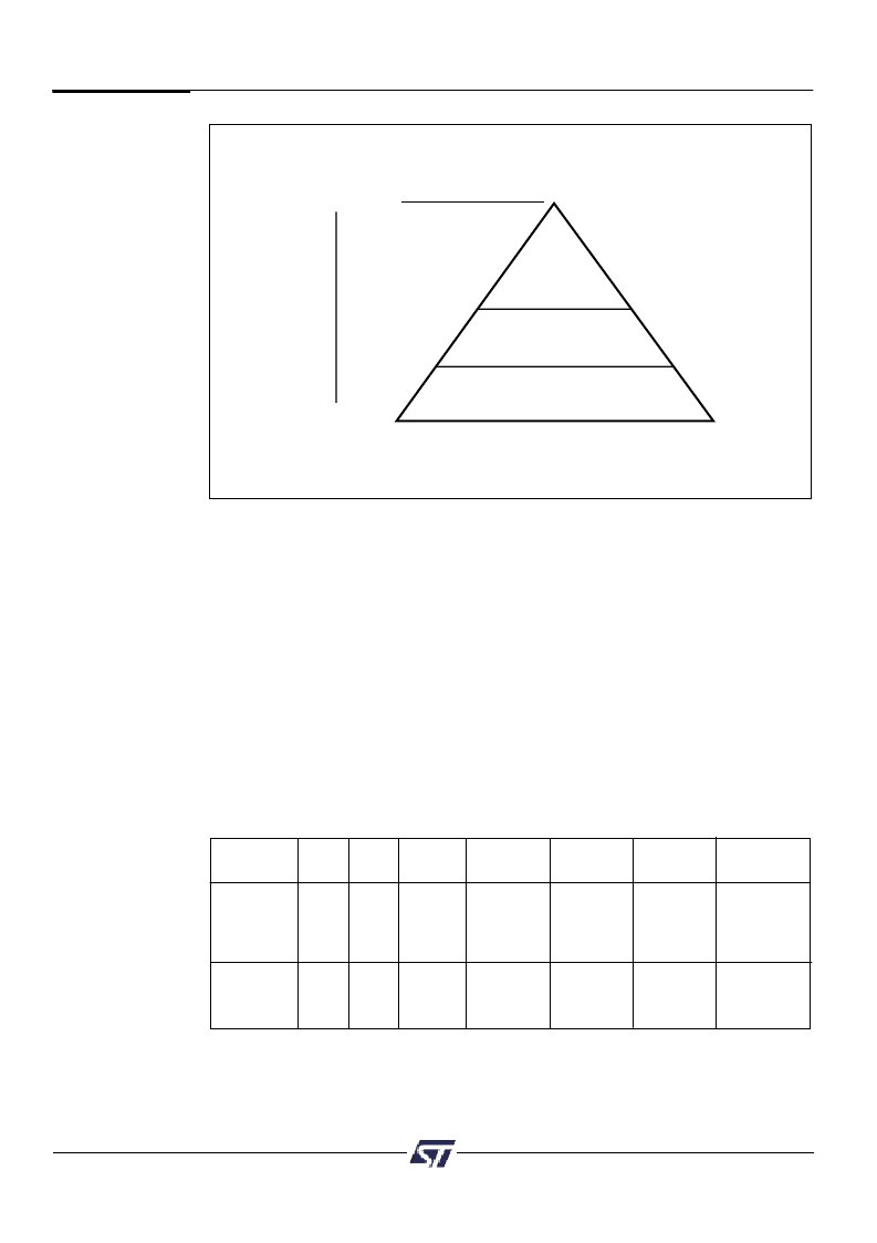
Level 1
SRAM, I/O
Level 2
Secondary Flash Memory
Highest Priority
Lowest Priority
Level 3
Main Flash Memory
Figure 6. Priority Level of Memory and I/OComponents
9.1.3.1. Memory Select Configuration for MCUs with Separate Program and Data Spaces
The 80C51 and compatible family of microcontrollers, can be configured to have separate
address spaces for code memory (selected using PSEN) and data memory (selected using
RD). Any of the memories within the PSD935G2 can reside in either space or both spaces.
This is controlled through manipulation of the VM register that resides in the PSD
’
s CSIOP
space.
The VM register is set using PSDsoft to have an initial value. It can subsequently be
changed by the microcontroller so that memory mapping can be changed on-the-fly.
For example, you may wish to have SRAM and main Flash in Data Space at boot, and
secondary Flash memory in Program Space at boot, and later swap main and secondary
Flash memory. This is easily done with the VM register by using PSDsoft to configure it for
boot up and having the microcontroller change it when desired.
Table 11 describes the VM Register.
Bit 7
PIO_EN
Bit 6* Bit 5*
Bit 4
FL_Data Boot_Data
Bit 3
Bit 2
FL_Code
Bit 1
Bit 0
Boot_Code SRAM_Code
0 = disable
PIO mode
*
*
0 = RD
can
’
t
access
Flash
0 = RD
can
’
t
access
Boot Flash
0 = PSEN
can
’
t
access
Flash
0 = PSEN
can
’
t
access
Boot Flash
0 = PSEN
can
’
t
access
SRAM
1= enable
PIO mode
*
*
1 = RD
access
Flash
1 = RD
access
Boot Flash
1 = PSEN
access
Flash
1 = PSEN
access
Boot Flash
1 = PSEN
access
SRAM
Table 11. VM Register
NOTE:
Bits 6-5 are not used.
發(fā)布緊急采購,3分鐘左右您將得到回復(fù)。