- 您現(xiàn)在的位置:買賣IC網(wǎng) > PDF目錄368341 > PT5062R Analog IC PDF資料下載
參數(shù)資料
| 型號: | PT5062R |
| 英文描述: | Analog IC |
| 中文描述: | 模擬IC |
| 文件頁數(shù): | 1/4頁 |
| 文件大小: | 114K |
| 代理商: | PT5062R |
For technical support and more information, see inside back cover or visit www.ti.com
Ordering Information
PT 5061
= ±12 Volts
PT 5062
= ±15 Volts
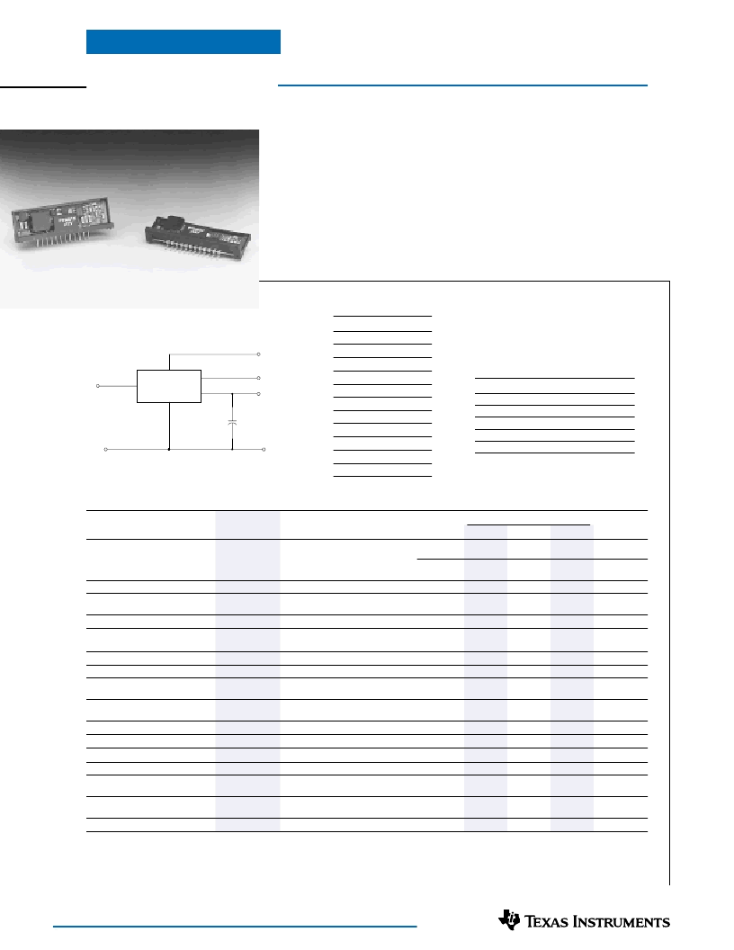
Standard Application
C
1
= Required 100μF electrolytic
Pin-Out Information
Pin
Function
1
–Vo
2
2
GND
3
V
in
4
V
in
5
V
in
6
GND
7
GND
8
+Vo
1
9
+Vo
1
10
+Vo
1
11
V
o
Adj
12
Do Not Connect
Features
Single Device:+5V Input
Complimentary Dual Output:
±12V, ±15V
Wide Input Voltage Range
85% Efficiency
Adjustable Output Voltage
Laser-trimmed
PT5060 Series
SLTS027B
(Revised 12/19/2001)
PT Series Suffix
(PT1234
x
)
Case/Pin
Configuration
Vertical
Horizontal
SMD
Vertical, Side Tabs
Horizontal, Side Tabs
SMD, Side Tabs
* Previously known as package style 300.
(Reference the applicable package code drawing
for the dimensions and PC board layout)
Order
Suffix
N
A
C
R
G
B
Package
C ode *
(ECD)
(ECA)
(ECC)
(ECE)
(ECG)
(ECK)
Description
The PT5060 series of dual-output
Integrated Switching Regulators (ISRs)
provide a complimentary ±12V or ±15V
from a single +5V input. Applications
include systems that require power for
analog interface circuitry, such as D/A
and A/D converters, and Op Amps. The
output voltage can be adjusted with an
external resistor. These ISRs are made
available in a 12-pin single in-line pin
(SIP) package. Note that these modules
are are not short-circuit protected.
9-W +5V-Input Dual-Output
Integrated Switching Regulator
Specifications
(Unless otherwise stated, T
a
=25°C, V
in
=+5V, I
o
=I
o
max, C
1
=100μF)
PT5060 SERIES
Typ
—
—
—
—
150
(2)
5.5
(3)
2
—
±1.5
±5
±0.5
±0.5
±1.5
±2
100
3
85
650
—
—
Characteristics
Output Current
Symbol
I
o
Conditions
Over V
in
range
Min
0.05
0.05
(1)
0.05
0.05
(1)
—
—
—
4.75
—
—
—
—
—
—
—
—
—
—
0
–40
Max
0.50
0.25
0.40
0.20
—
—
—
+V
o
–1
±3.0
±10
±1.0
±1.0
±3
±3
—
5
—
—
+85
(4)
+125
Units
Vo
1
= +12V
Vo
2
= –12V
Vo
1
= +15V
Vo
2
= –15V
A
A
Current Limit
Inrush Current
I
lim
I
ir
t
tr
V
in
V
o
%I
o
max
A
mSec
V
On start up
Input Voltage Range
Output Voltage Tolerance
Over I
o
range
Over V
and I
ranges
T
a
= 0°C to SOA limit
(3)
Over V
in
range
0.1
≤
I
o
≤
I
o
max
20MHz bandwidth
+Vo
1
–Vo
2
%V
o
Line Regulation
Load Regulation
V
o
Ripple (pk-pk)
Reg
line
Reg
load
V
n
%V
o
%V
o
+Vo
1
–Vo
2
%V
o
Transient Response
t
tr
V
os
η
s
T
a
T
s
25% load change
V
o
over/undershoot
I
o
=0.2A each output
Over V
in
and I
o
ranges
—
μSec
%V
o
%
kHz
°C
°C
Efficiency
Switching Frequency
Operating Temperature Range
Storage Temperature
Mechanical Shock
Per Mil-STD-883D, Method 2002.3,
1 msec, Half Sine, mounted to a fixture
Per Mil-STD-883D, Method 2007.2
20-2000 Hz, Soldered in a PC board
—
500
—
G’s
Mechanical Vibration
—
15
—
G’s
Weight
—
6.5
—
grams
Notes:
(1) Do not operate thes negative output rail of these ISRs below the minimum load.
(2) ISRs based on a boost topology are not short-circuit protected.
(3) The inrush current stated is above the normal input current for the associated output load.
(4) See Safe Operating Area curves or consult the factory for the appropriate derating
.
C
1
100
μ
F
+
–Vo
2
COM
Vin
COM
+Vo
1
PT5060
1
2,6,7
3,4,5
11
8,9,10
V
o
adj
相關(guān)PDF資料 |
PDF描述 |
|---|---|
| PT5061A | 30V Single N-Channel HEXFET Power MOSFET in a D2-Pak package; A IRL3803S with Standard Packaging |
| PT5061B | Analog IC |
| PT5061C | Analog IC |
| PT5061G | Analog IC |
| PT5061N | 100V Single N-Channel HEXFET Power MOSFET in a TO-220AB package; A IRF540NPBF with Standard Packaging |
相關(guān)代理商/技術(shù)參數(shù) |
參數(shù)描述 |
|---|---|
| PT5065 | 功能描述:變壓器音頻和信號 ISDN U XFMR;SGS TH & NAT’L;RM CORE RoHS:否 制造商:Skyworks Solutions, Inc. 頻率范圍:810 MHz to 960 MHz 初級線圈阻抗: 次級線圈阻抗: 絕緣電壓:23 dB 工作溫度范圍:- 40 C to + 85 C 端接類型:SMD/SMT 尺寸:6 mm L x 4.9 mm W x 1.6 mm H 產(chǎn)品:Splitters and Combiners |
| PT506-5 | 制造商:未知廠家 制造商全稱:未知廠家 功能描述:TRIAC|500V V(DRM)|6A I(T)RMS|TO-5VAR |
| PT506-66 | 制造商:未知廠家 制造商全稱:未知廠家 功能描述:TRIAC|500V V(DRM)|6A I(T)RMS|TO-66 |
| PT5069 | 功能描述:變壓器音頻和信號 ISDN DUAL XFMR RoHS:否 制造商:Skyworks Solutions, Inc. 頻率范圍:810 MHz to 960 MHz 初級線圈阻抗: 次級線圈阻抗: 絕緣電壓:23 dB 工作溫度范圍:- 40 C to + 85 C 端接類型:SMD/SMT 尺寸:6 mm L x 4.9 mm W x 1.6 mm H 產(chǎn)品:Splitters and Combiners |
| PT506S | 制造商:未知廠家 制造商全稱:未知廠家 功能描述:TRIAC|500V V(DRM)|6A I(T)RMS|TO-208VAR1/2 |
發(fā)布緊急采購,3分鐘左右您將得到回復(fù)。