- 您現(xiàn)在的位置:買賣IC網(wǎng) > PDF目錄98065 > PTH12010LAZ (TEXAS INSTRUMENTS INC) 1-OUTPUT DC-DC REG PWR SUPPLY MODULE PDF資料下載
參數(shù)資料
| 型號: | PTH12010LAZ |
| 廠商: | TEXAS INSTRUMENTS INC |
| 元件分類: | 電源模塊 |
| 英文描述: | 1-OUTPUT DC-DC REG PWR SUPPLY MODULE |
| 封裝: | ROHS COMPLIANT, DIP-10 |
| 文件頁數(shù): | 21/27頁 |
| 文件大?。?/td> | 931K |
| 代理商: | PTH12010LAZ |
第1頁第2頁第3頁第4頁第5頁第6頁第7頁第8頁第9頁第10頁第11頁第12頁第13頁第14頁第15頁第16頁第17頁第18頁第19頁第20頁當前第21頁第22頁第23頁第24頁第25頁第26頁第27頁
www.ti.com
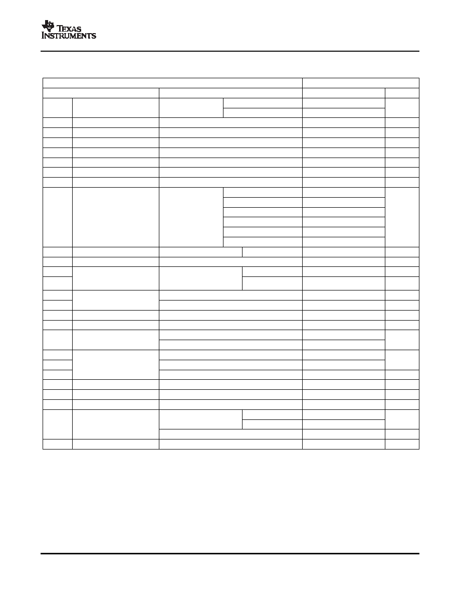
ELECTRICAL CHARACTERISTICS
SLTS205G – JUNE 2003 – REVISED FEBRUARY 2007
T
A = 25°C, VI = 12 V, VO = 3.3 V, CI = 560 F, CO = 0 F, and IO = IO max (Unless otherwise stated)
PTH12010W
CHARACTERISTICS
CONDITIONS
MIN
TYP
MAX
UNIT
60
°C, 200 LFM airflow
0
12(1)
Io
Output current
1.2 V
≤ V
o≤ 5.5 V
A
25
°C, natural convection
0
12(1)
VI
Input voltage range
Over Io range
10.8
13.2
V
Vo tol
Set-point voltage tolerance
±2(2)
%Vo
Regtemp Temperature variation
–40 °C < TA < 85 °C
±0.5
%Vo
Regline
Line regulation
Over VI range
±10
mV
Regload
Load regulation
Over Io range
±12
mV
Regtot
Total output variation
Includes set-point, line, load, –40°C
≤ T
A ≤ 85°C
±3(2)
%Vo
Vadj
Output voltage adjust range
Over VI range
1.2
5.5
V
RSET = 280 , Vo = 5V
94
RSET = 2.0 k, Vo = 3.3V
93
RSET = 4.32 k, Vo = 2.5V
91
η
Efficiency
IO = 8 A
%
RSET = 11.5 k, Vo = 1.8V
89
RSET = 24.3 k, Vo = 1.5V
88
RSET = OPEN, Vo
86
Vr
VO ripple (peak-to-peak)
20-MHz bandwidth
All Vo
1
% VO
Io trip
Overcurrent threshold
Reset, followed by auto-recovery
20
A
ttr
1 A/s load step,
Recovery Time
70
Sec
Transient response
50 to 100% Iomax,
Vo over/undershoot
100
mV
Vtr
CO= 330 F
VOmargin
Margin up/down adjust
±5
%
Margin Control
(pins 9 &10)
IILmargin
Margin input current, Pin to GND
–8(3)
A
IILtrack
Track input current (pin 8)
Pin to GND
–0.13(4)
mA
dVtrack/dt Track slew rate capability
CO≤ CO(max)
1
V/ms
VI increasing
9.5
10.4
UVLO
Undervoltage lockout
V
VI decreasing
8.8
9
VIH
Input high voltage, Referenced to GND
Open(4)
V
VIL
Inhibit control (pin 3)
Input low voltage, Referenced to GND
–0.2
0.5
IIL
Input low current, Pin 3 to GND
0.24
mA
II
Input standby current
Inhibit (pin 3) to GND, Track (pin 8) open
10
mA
fs
Switching frequency
Over VI and Io ranges
300
350
400
kHz
CI
External input capacitance
560(5)
F
nonceramic
0(6)
330(7)
6,600(8)
Capacitance value
F
CO
External output capacitance
ceramic
0
300
Equivalent series resistance (nonceramic)
4(9)
m
MTBF
Reliability
Bellcore TR-332,50% stress,TA=40°C, GND benign
6.4
106 Hr
(1)
See SOA curves or consult factory for appropriate derating.
(2)
The set-point voltage tolerance is affected by the tolerance and stability of RSET. The stated limit is unconditionally met if RSET has a
tolerance of 1%, with 100 ppm/
°C (or better) temperature stability.
(3)
A small, low-leakage (<100 nA) MOSFET is recommended to control this pin. The open-circuit voltage is less than 1 Vdc.
(4)
This control pin has an internal pull-up to the input voltage VI (7.5 V for pin 8). If it is left open-circuit the module operates when input
power is applied. A small, low-leakage (<100 nA) MOSFET or open-drain/collector voltage supervisor IC is recommended for control. Do
not place an external pull-up on this pin. For further information, see the related application section.
(5)
A 560
F electrolytic input capacitor, rated for a minimum of 800 mA rms of ripple current is required for proper operation.
(6)
When operating at an output voltage
≥ 3.3 V, 47-F of external output capacitance is required for proper operation.
(7)
External output capacitance is not required for operation. Adding 330
F of distributed capacitance improves the transient response.
(8)
This is the calculated maximum. The minimum ESR limitation often results in a lower value. When controlling the Track pin using a
voltage supervisor, CO(max) is reduced to 3300 F. See the application notes for further guidance.
(9)
This is the typical ESR for all nonceramic ouput capacitance. Use 7 m
as the minimum when using max-ESR values to calculate.
3
相關PDF資料 |
PDF描述 |
|---|---|
| PTH12010WAST | 1-OUTPUT DC-DC REG PWR SUPPLY MODULE |
| PTH12030WAZT | 1-OUTPUT DC-DC REG PWR SUPPLY MODULE |
| PTH12030WAZ | 1-OUTPUT DC-DC REG PWR SUPPLY MODULE |
| PTH12030LAH | 1-OUTPUT DC-DC REG PWR SUPPLY MODULE |
| PTH12030WAS | 1-OUTPUT DC-DC REG PWR SUPPLY MODULE |
相關代理商/技術參數(shù) |
參數(shù)描述 |
|---|---|
| PTH12010LAZT | 功能描述:DC/DC轉換器 0.8 to 1.8V 12A 12V Input WideAdj Module RoHS:否 制造商:Murata 產品: 輸出功率: 輸入電壓范圍:3.6 V to 5.5 V 輸入電壓(標稱): 輸出端數(shù)量:1 輸出電壓(通道 1):3.3 V 輸出電流(通道 1):600 mA 輸出電壓(通道 2): 輸出電流(通道 2): 安裝風格:SMD/SMT 封裝 / 箱體尺寸: |
| PTH12010W | 制造商:TI 制造商全稱:Texas Instruments 功能描述:12-A, 12-V INPUT NON-ISOLATED WIDE-OUTPUT ADJUST POWER MODULE |
| PTH12010WAD | 功能描述:DC/DC轉換器 10.8-13.2Vin 5.5V12A 1.370" x0.620"x0.354 RoHS:否 制造商:Murata 產品: 輸出功率: 輸入電壓范圍:3.6 V to 5.5 V 輸入電壓(標稱): 輸出端數(shù)量:1 輸出電壓(通道 1):3.3 V 輸出電流(通道 1):600 mA 輸出電壓(通道 2): 輸出電流(通道 2): 安裝風格:SMD/SMT 封裝 / 箱體尺寸: |
| PTH12010WADT | 制造商:EMERSON-NETWORKPOWER 制造商全稱:Emerson Network Power 功能描述:DC-DC CONVERTERS |
| PTH12010WAH | 功能描述:DC/DC轉換器 1.2 to 5.5V 12A 12V Input WideAdj Module RoHS:否 制造商:Murata 產品: 輸出功率: 輸入電壓范圍:3.6 V to 5.5 V 輸入電壓(標稱): 輸出端數(shù)量:1 輸出電壓(通道 1):3.3 V 輸出電流(通道 1):600 mA 輸出電壓(通道 2): 輸出電流(通道 2): 安裝風格:SMD/SMT 封裝 / 箱體尺寸: |
發(fā)布緊急采購,3分鐘左右您將得到回復。