- 您現(xiàn)在的位置:買賣IC網(wǎng) > PDF目錄368355 > PTH12030W Universal Input Linear Fluorescent Ballast using the IR2167 PDF資料下載
參數(shù)資料
| 型號: | PTH12030W |
| 英文描述: | Universal Input Linear Fluorescent Ballast using the IR2167 |
| 中文描述: | 26答:12 - V輸入寬輸出調(diào)節(jié)插入電源模塊 |
| 文件頁數(shù): | 3/8頁 |
| 文件大小: | 171K |
| 代理商: | PTH12030W |
A
For technical support and more information, see inside back cover or visit www.ti.com
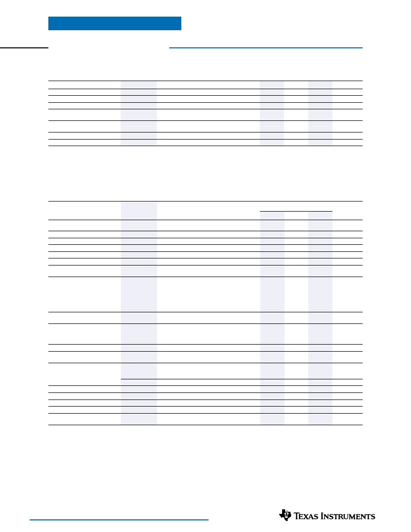
Environmental & Absolute Maximum Ratings
(Voltages are with respect to GND)
Characteristics
Symbols
Conditions
Min
Typ
Max
Units
Operating Temperature Range
Solder Reflow Temperature
Storage Temperature
Mechanical Shock
T
a
T
reflow
T
s
Over V
in
Range
Surface temperature of module body or pins
—
Per Mil-STD-883D, Method 2002.3
1 msec, sine, mounted
Mil-STD-883D, Method 2007.2
20-2000 Hz
–40
(i)
—
+85
215
(ii)
+125
°C
°C
°C
–40
—
—
TBD
—
G’s
Mechanical Vibration
—
TBD
—
G’s
Weight
Flammability
—
—
—
2
—
grams
Meets UL 94V-O
Notes:
(i) For operation below 0 °C the external capacitors must have stable characteristics. Use either a low ESR tantalum or Oscon capacitor.
(ii) During reflow of SMD package version do not elevate peak temperature of the module, pins or internal components above the stated maximum. For
further guidance refer to the application note, “Reflow Soldering Requirements for Plug-in Power Surface Mount Products.”
Electrical Specifications
Unless otherwise stated, T
a
=25 °C, V
in
=12 V, V
out
=3.3 V, C
in
=100 μF, C
out
=0 μF, and I
o
=I
o
max
PTH12000W
Typ
Characteristics
Symbols
Conditions
Min
Max
Units
Output Current
I
o
T
a
=60 °C, 200 LFM
T
a
=25 °C, natural convection
Over I
o
range
0
0
10.8
—
—
—
—
—
—
—
—
±0.5
±5
±5
6
(1)
6
(1)
13.2
±2
—
—
—
A
Input Voltage Range
Set-Point Voltage Tolerance
Temperature Variation
Line Regulation
Load Regulation
Total Output Variation
V
in
V
o
tol
Reg
temp
Reg
line
Reg
load
Reg
tot
V
%V
o
%V
o
mV
mV
–40 °C <T
a
< +85 °C
Over V
in
range
Over I
o
range
Includes set-point, line, load,
–40 °C
≤
T
a
≤
+85 °C
V
in
=12 V, I
o
=4 A
—
—
±3
%V
o
Efficiency
η
R
SET
= 280
R
SET
= 2.0 k
R
SET
= 4.32 k
V
o
=
R
SET
= 8.06 k
V
o
=
2.0 V
R
SET
= 11.5 k
V
o
=
1.8 V
R
SET
= 24.3 k
V
o
=
1.5 V
R
SET
= open cct V
o
=
1.2 V
V
o
=
5.0 V
V
o
=
2.5 V
—
—
—
—
—
—
—
—
—
92
90
88
87
86
84
82
50
30
—
—
—
—
—
—
—
—
—
%
V
o
Ripple (pk-pk)
V
r
20 MHz bandwidth, I
o
=4 A
V
o
≥
3.3 V
V
o
≤
2.5 V
mVpp
Transient Response
1 A/μs load step, 50 to 100 % I
o
max,
V
=1.8 V, C
out
=100 μF
Recovery time
V
o
over/undershoot
Reset followed by auto-recovery
V
in
increasing
V
in
decreasing
Referenced to GND
t
tr
V
tr
I
o
trip
UVLO
—
—
—
—
8.8
70
100
12
—
—
—
—
—
10.4
—
μSec
mV
A
Over-Current Threshold
Under-Voltage Lockout
V
Inhibit Control (pin 3)
Input High Voltage
Input Low Voltage
Input Low Current
Standby Input Current
Switching Frequency
External Input Capacitance
External Output Capacitance
Reliability
V
IH
V
IL
I
IL
I
in
standby
s
C
in
C
out
MTBF
V
–0.5
–0.2
—
—
—
100
(3)
0
—
—
–240
1
350
—
100
(4)
Open
(2)
0.5
—
—
—
—
TBD
V
Pin 3 to GND
pins 1 & 3 connected
Over V
in
and I
o
ranges
μA
mA
kHz
μF
μF
Per Bellcore TR-332
50 % stress, T
a
=40 °C, ground benign
10
—
—
10
6
Hrs
Notes:
(1) See SOA curves or consult factory for appropriate derating.
(2) The Inhibit control (pin 3) has an internal pull-up to Vin, and if left open-circuit the module will operate when input power is applied. A small low-
leakage (<100 nA) MOSFET is recommended to control this input. See application notes for more information.
(3) The regulator requires a minimum of 100 μF input capacitor with a minimum 750 mArms ripple current rating. For further information, consult the
related application note on Capacitor Recommendations.
(4) An external output capacitor is not required for basic operation. Adding 100 μF of distributed capacitance at the load will improve the transient response.
6-A, 12-V Input Non-Isolated
Wide-Output Adjust Power Module
SLTS202A
–
MAY 2003
–
REVISED MAY 2003
PTH12000 Series
—
12-V Input
相關(guān)PDF資料 |
PDF描述 |
|---|---|
| PTH8C16TBB101M | Universal Input Linear Fluorescent Ballast using the IR2166 |
| PTH8C16TBB221M | Mini-ballast for single 25W compact fluorescent ballast, European version with 230VACin |
| PTH8C16TBB330M | Intelligent Power Switch 1 Channel Low Side Driver in a SOT-223 Package |
| PTH8C16TBB470M | Intelligent Power Switch 1 Channel Low Side Driver in a TO-220AB Package |
| PTH8C16TBB481M | Intelligent Power Switch 1 Channel Low Side Driver in a SOT-223 Package |
相關(guān)代理商/技術(shù)參數(shù) |
參數(shù)描述 |
|---|---|
| PTH12030WAD | 功能描述:DC/DC轉(zhuǎn)換器 1.2 to 5.5V 26A 12V Input WideAdj Module RoHS:否 制造商:Murata 產(chǎn)品: 輸出功率: 輸入電壓范圍:3.6 V to 5.5 V 輸入電壓(標(biāo)稱): 輸出端數(shù)量:1 輸出電壓(通道 1):3.3 V 輸出電流(通道 1):600 mA 輸出電壓(通道 2): 輸出電流(通道 2): 安裝風(fēng)格:SMD/SMT 封裝 / 箱體尺寸: |
| PTH12030WADT | 制造商:EMERSON-NETWORKPOWER 制造商全稱:Emerson Network Power 功能描述:DC-DC CONVERTERS |
| PTH12030WAH | 功能描述:DC/DC轉(zhuǎn)換器 1.2 to 5.5V 26A 12V Input WideAdj Module RoHS:否 制造商:Murata 產(chǎn)品: 輸出功率: 輸入電壓范圍:3.6 V to 5.5 V 輸入電壓(標(biāo)稱): 輸出端數(shù)量:1 輸出電壓(通道 1):3.3 V 輸出電流(通道 1):600 mA 輸出電壓(通道 2): 輸出電流(通道 2): 安裝風(fēng)格:SMD/SMT 封裝 / 箱體尺寸: |
| PTH12030WAH | 制造商:POWER TRENDS 功能描述:IC DC/DC 12VIN 26A ADJ O/P 12030 |
| PTH12030WAHT | 制造商:EMERSON-NETWORKPOWER 制造商全稱:Emerson Network Power 功能描述:DC-DC CONVERTERS |
發(fā)布緊急采購,3分鐘左右您將得到回復(fù)。