- 您現(xiàn)在的位置:買賣IC網(wǎng) > PDF目錄361302 > QMR1 (Electronic Theatre Controls, Inc.) QM Receiver Module PDF資料下載
參數(shù)資料
| 型號: | QMR1 |
| 廠商: | Electronic Theatre Controls, Inc. |
| 英文描述: | QM Receiver Module |
| 中文描述: | 質(zhì)量管理接收模塊 |
| 文件頁數(shù): | 3/8頁 |
| 文件大小: | 97K |
| 代理商: | QMR1 |

Ds302_3 AUG 01
ó
2001 REG No 277 4001 England
Page 3
QM Receiver Module QMR1 / QMR2
QMR1 Details
QMR1
1
2
3
4
5
6
7
Figure 1: QMR1 Receiver
Pin Description:
Vcc ( PIN 1 )
+Ve supply pin. Operation from a 5V supply able
to source 2mA at less than 10mV
P-P
ripple.
GND ( PIN 2 )
Supply ground connection, preferably connected
to a solid ground plane.
RF IN ( PIN 3 )
50
RF input from antenna, connect using
shortest possible route. Capacitively isolated from
internal circuit.
UNCONNECTED ( PINS 4 & 5 )
Extra SIL pins for additional mechanical retention.
RSSI
( PIN 6 )
Test output providing a voltage that is proportional
to the level of the RF input on pin 3.
DATA OUT ( PIN 7 )
CMOS compatible output. This may be used to
drive external decoders.
Note:
sink/source
capability is limited to 20
μ
A.
General Information
Phase
Lock
Loop
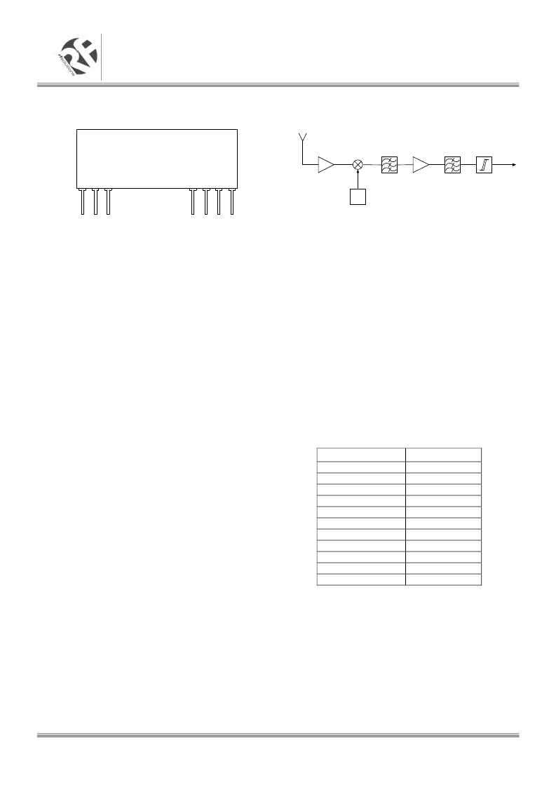
RF
Band Pass
Filter
IF
Low Pass
Filter
Detector
Antenna
Mixer
Figure 2: Receiver Block Diagram
The receiver module is a quasi AM /FM (QM)
superhet receiver capable of handling data rates
of up to 10Kbits/s. With an on board data buffer
and phase locked loop a –110 dBm sensitivity is
achieved.
Utilising the quasi AM/FM modulation technique
and the latest phase locked loop receiver
technology with one of the compatible transmitter
modules will yield a highly efficient wireless link.
Note:
Because of the way Quasi Modulation
operates the QMR1 and the QFMT1 will not work
reliably in close proximity to each other.
RSSI Values
RF Level (dBm) pin 3
RSSI (volts) pin 6
-110
2.12
-100
2.21
-90
2.31
-80
2.46
-70
2.62
-60
2.80
-50
2.91
-40
2.97
-30
3.00
-20
3.03
-10
2.88
相關(guān)PDF資料 |
PDF描述 |
|---|---|
| QMR1-434 | QM Receiver Module |
| QMR1-868 | QM Receiver Module |
| QMR2-434 | QM Receiver Module |
| QN89027 | MODEM CIRCUIT|ANALOG FRONT END|CMOS|LDCC|28PIN|PLASTIC |
| QP89027 | MODEM CIRCUIT|ANALOG FRONT END|CMOS|DIP|28PIN|PLASTIC |
相關(guān)代理商/技術(shù)參數(shù) |
參數(shù)描述 |
|---|---|
| QMR110 | 制造商:QUALTEK 制造商全稱:QUALTEK 功能描述:MOLDED PARTS |
| QMR120 | 制造商:QUALTEK 制造商全稱:QUALTEK 功能描述:MOLDED PARTS |
| QMR130 | 制造商:QUALTEK 制造商全稱:QUALTEK 功能描述:MOLDED PARTS |
| QMR140 | 制造商:QUALTEK 制造商全稱:QUALTEK 功能描述:MOLDED PARTS |
| QMR1-434 | 制造商:RFSOLUTIONS 制造商全稱:rfsolutions.ltd 功能描述:QM Receiver Module |
發(fā)布緊急采購,3分鐘左右您將得到回復(fù)。