- 您現(xiàn)在的位置:買賣IC網(wǎng) > PDF目錄361315 > QS532806ASO Five Distributed-Output Clock Driver PDF資料下載
參數(shù)資料
| 型號(hào): | QS532806ASO |
| 英文描述: | Five Distributed-Output Clock Driver |
| 中文描述: | 五分布式輸出時(shí)鐘驅(qū)動(dòng)器 |
| 文件頁(yè)數(shù): | 3/6頁(yè) |
| 文件大小: | 95K |
| 代理商: | QS532806ASO |

3
QS532806/A
GUARANTEED LOW SKEW 3.3V CMOS CLOCK DRIVER/BUFFER
INDUSTRIAL TEMPERATURE RANGE
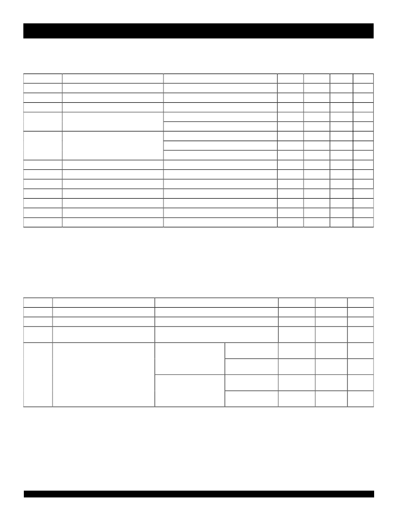
DC ELECTRICAL CHARACTERISTICS OVER OPERATING RANGE
Following Conditions Apply Unless Otherwise Specified:
Industrial: T
A
= -40°C to +85°C, V
CC
= 3.3V ± 0.3V
Symbol
V
IH
V
IL
V
IC
V
OH
Parameter
Test Conditions
Mn.
2
–0.5
—
Typ.
(1)
—
—
–0.7
—
—
—
—
—
—
—
—
–100
100
—
28
Max.
5.5
0.8
–1.2
—
—
0.2
0.4
0.5
±1
±1
±1
–200
200
—
—
Unit
V
V
V
V
V
V
V
V
μ
A
μ
A
μ
A
mA
mA
mA
Input HIGH Voltage
Input LOW Voltage
Clamp Diode Voltage
(3)
Output HIGH Voltage
Guaranteed Logic HIGH for Inputs
Guaranteed Logic LOW for Inputs
Vcc = Mn., I
IN
= -18mA
Vcc = Mn., I
OH
= -100
μ
A
Vcc = Mn., I
OH
= -8mA
Vcc = Mn., I
OL
= 100
μ
A
Vcc = Mn., I
OL
= 6mA
Vcc = Mn., I
OL
= 8mA
Vcc = Max., V
IN
= Vcc or GND
Vcc = Max., V
OUT
= Vcc or GND
Vcc = 0V, V
IN
= Vcc or GND
Vcc = 3.3V, V
IN
= V
IH
or V
IL
, V
O
= 1.5V
Vcc = 3.3V, V
IN
= V
IH
or V
IL
, V
O
= 1.5V
Vcc = Max., V
OUT
= GND
Vcc = Mn
Vcc – 0.2
2.4
—
—
—
—
—
—
–30
30
–
60
—
V
OL
Output LOW Voltage
I
IN
I
OZ
I
OFF
I
ODH
I
ODL
I
OS
R
OUT
Input Leakage Current
Output Leakage Current
Input Power Off Leakage
Output HIGH Current
(2)
Output LOW Current
(2)
Short Circuit Current
(2,3)
Output Resistance
(4)
NOTES:
1. Typical values are at V
CC
= 3.3V, T
A
= 25°C.
2. Not more than one output should be used to test this high power condition. Duration is less than one second.
3. Guaranteed by design but not tested.
4. Output resistance represents the total output impedence of the logic device and includes added series termination resistance.
POWER SUPPLY CHARACTERISTICS
Symbol
I
CC
I
CC
I
CCD
Parameter
Test Conditions
(1)
Typ.
(3)
0.01
0.1
65
Max.
100
30
100
Unit
μ
A
μ
A
μ
A/MHz
Quiescent Power Supply Current
Supply Current per Input HIGH
Dynamc Power Supply Current per Output
(2)
V
CC
= Max., V
IN
= GND or Vcc
V
CC
= Max., V
IN
= 3V
V
CC
= Max.,
OEA
=
OEB
= GND
Outputs Toggling at 50% duty cycle
V
CC
= Max.,
OEA
=
OEB
= GND
50% duty cycle, f
I
= 10MHz
five outputs
V
CC
= Max.,
OEA
=
OEB
= GND
50% duty cycle, f
I
= 2.5MHz
All outputs toggling
I
C
Total Power Supply Current Examples
(2,4)
V
IN
= GND or Vcc
3.5
5.2
mA
V
IN
= GND or 3V
3.5
5.2
mA
V
IN
= GND or Vcc
1.8
2.9
mA
V
IN
= GND or 3V
1.8
2.9
mA
NOTES:
1. For conditions shown as Min. or Max., use the appropriate values specified under DC Electrical Characteristics.
2. Guaranteed by design but not tested. C
L
= 0pF.
3. Typical values are for reference only. Conditions are V
CC
= 3.3V, T
A
= 25°C.
4. I
C
= I
CC
+ (
I
CC
)(D
H
)(N
T
) + I
CCD
(f
O
)(N
O
)
where:
D
H
= Input Duty Cycle
N
T
= Number of TTL HIGH inputs at D
H
(one or two)
f
O
= Output Frequency
N
O
= Number of outputs at f
O
(five or ten)
相關(guān)PDF資料 |
PDF描述 |
|---|---|
| QS532807AQ | Ten Distributed-Output Clock Driver |
| QS532807ASO | Ten Distributed-Output Clock Driver |
| QS53807AQ | Ten Distributed-Output Clock Driver |
| QS53807ASO | Ten Distributed-Output Clock Driver |
| QS53807Q | Ten Distributed-Output Clock Driver |
相關(guān)代理商/技術(shù)參數(shù) |
參數(shù)描述 |
|---|---|
| QS532807 | 制造商:IDT 制造商全稱:Integrated Device Technology 功能描述:GUARANTEED LOW SKEW CMOS CLOCK DRIVER/BUFFER |
| QS532807AQ | 制造商:未知廠家 制造商全稱:未知廠家 功能描述:Ten Distributed-Output Clock Driver |
| QS532807ASO | 制造商:未知廠家 制造商全稱:未知廠家 功能描述:Ten Distributed-Output Clock Driver |
| QS532807Q | 制造商:IDT 制造商全稱:Integrated Device Technology 功能描述:GUARANTEED LOW SKEW CMOS CLOCK DRIVER/BUFFER |
| QS532807SO | 制造商: 功能描述: 制造商:undefined 功能描述: |
發(fā)布緊急采購(gòu),3分鐘左右您將得到回復(fù)。