- 您現(xiàn)在的位置:買賣IC網(wǎng) > PDF目錄373223 > R1250V3.91A-E2 Analog IC PDF資料下載
參數(shù)資料
| 型號: | R1250V3.91A-E2 |
| 英文描述: | Analog IC |
| 中文描述: | 模擬IC |
| 文件頁數(shù): | 12/13頁 |
| 文件大小: | 127K |
| 代理商: | R1250V3.91A-E2 |
12345
Rev. 1.10 - 12 -
n
OPERATION
1) Basic Operation
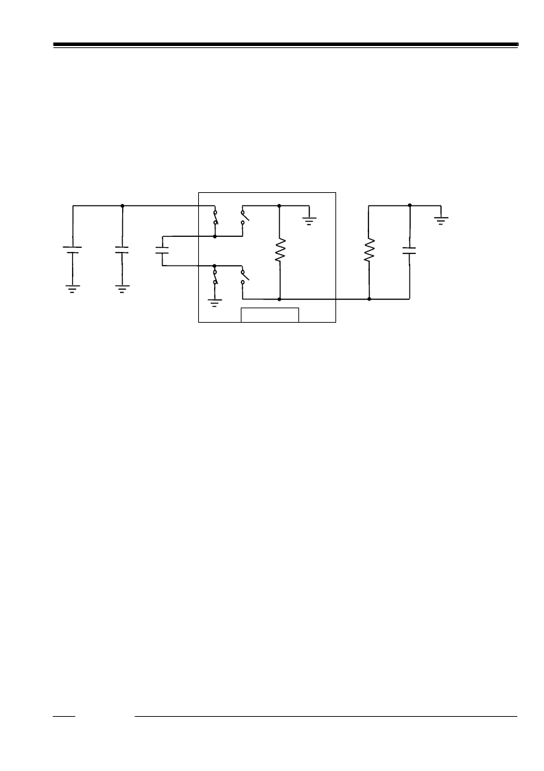
The R1250Vxx1A Series make SW1 through SW4 ON and OFF by the clock generated by internal oscillator (OSC)
with fixed frequency, and operate as a inverting charge pump with the capacitor C
P
and the capacitor C
OUT.
The Output Voltage is feedback and the voltage between the Output Voltage and Reference Voltage (V
REF
=
V
OUT
V) is divided half, and it is compared with the GND (=0V) level by an internal operational amplifier.
By this action, the impedance of SW3 is controlled to correspond with its load current and Output Voltage keeps
“
Set V
OUT
” level.
2) Status of Internal Circuits at Standby mode and Standby Current
At Standby mode, R1250V Series keep the voltage of C
P
as shown below:
R1250V301
V
IN
C
P
C
IN
up to 5k
W
R
OUT
C
OUT
V
OUT
When you design a system with using this IC, consider the following subjects;
2-(1) If very small leakage current would be a critical, the leakage current of both C
IN
and C
P
should be considered.
2-(2) Because the voltage level of C
P
keeps as much as V
DD
level, the speed for start-up from stand-by mode is faster
than the start-up by power-on.
2-(3) V
OUT
is internally pulled down through 5k
W
to GND. Time constant “
t
” of transient response (turn-off speed) of
V
OUT
can be calculated as follows:
t
@
(5[k
W
]
R
OUT
)
′
C
OUT (
R
OUT
: Output load resistance)
2-(4) Load current should be OFF synchronously with this IC if the load is electronic or connected between V
IN
and
V
OUT
. If some charge is continuously flown to the Output V
OUT
at the “OFF” state, the voltage level of V
OUT
will rise
and could be beyond 0V. And if the voltage will be +0.3V (that is designated as absolute maximum rating.), this IC
might be break down.
3) Ripple Voltage
Ripple voltage of Output waveform can be roughly calculated as follows:
Vripple [mVp-p]
@
0.5
′
(I
OUT
[mA] + Supply Current at no load [mA]) / (Oscillator Frequency: 280000 [Hz]) / C
OUT
[F]
Supply Current at no load [mA]
@
Supply Current 1 [mA]
4) Power Consumption
Power Consumption at large load current of this IC can be calculated as follows:
Wchip[mW]
@
(V
IN
[V]-| Set Output Voltage |)
′
(I
OUT
[mA])
n
TECHNICAL NOTES
To use this IC, the following things should be considered.
1) Short Protection function for each pin is not included in this IC.
2) Use capacitors with low equivalent series resistor (ESR) for C
IN
, C
P
, C
OUT
pins. Capacitors with large ESR make
this IC’s performance worse.
3) Make wiring of GND, V
IN
, C
P+
, C
P-
secure enough and decrease impedance. High impedance could be a cause of
unstable operation of this IC.
4) When this IC is used with large load current, consider its radiation of heat.
5) Basically, V
REF
pin can be used for soldering to the mount pad of PCB. Do not make it wiring.
6) Load type is electronic or setting between V
IN
and V
OUT
, in cases of OFF-state of this IC and start-up state of this
IC, make sure not to raise V
OUT
level on positive voltage side. If the voltage level is beyond +0.3V, which is
相關(guān)PDF資料 |
PDF描述 |
|---|---|
| R1250V4.01A- | Analog IC |
| R1250 | Linear Sensor Photodiode Array; 128x1 Sensor-Elements Organization; 400 Dots-Per-Inch (DPI) Sensor Pitch; High Linearity and Uniformity; Wide Dynamic Range 4000:1 (72 dB); Low Image Lag 0.5% Typ; Operation to 8MHz |
| R13-104A-01 | SWITCH ROCKER BLACK DPST |
| R13-104B-01 | SWITCH ROCKER ILLUM RED DPST |
| R13-104D-01 | SWITCH ROCKER BLACK DPDT |
相關(guān)代理商/技術(shù)參數(shù) |
參數(shù)描述 |
|---|---|
| R1250V4.01A- | 制造商:未知廠家 制造商全稱:未知廠家 功能描述:Analog IC |
| R1250V4.01A-E2 | 制造商:未知廠家 制造商全稱:未知廠家 功能描述:Analog IC |
| R1250V401A | 制造商:RICOH 制造商全稱:RICOH electronics devices division 功能描述:Negative Output Charge Pump Regulator |
| R1250V401A-E2 | 制造商:RICOH 制造商全稱:RICOH electronics devices division 功能描述:Negative Output Charge Pump Regulator(100mA) |
| R1250VXX1A | 制造商:RICOH 制造商全稱:RICOH electronics devices division 功能描述:Negative Output Charge Pump Regulator |
發(fā)布緊急采購,3分鐘左右您將得到回復(fù)。