- 您現(xiàn)在的位置:買賣IC網(wǎng) > PDF目錄296949 > R1283Z002A-E2-F (RICOH COMPANY LTD) DC-DC REG PWR SUPPLY MODULE PDF資料下載
參數(shù)資料
| 型號: | R1283Z002A-E2-F |
| 廠商: | RICOH COMPANY LTD |
| 元件分類: | 電源模塊 |
| 英文描述: | DC-DC REG PWR SUPPLY MODULE |
| 封裝: | MODULE-11 |
| 文件頁數(shù): | 1/2頁 |
| 文件大小: | 229K |
| 代理商: | R1283Z002A-E2-F |
R1283x Series
PWM Step-up/Inverting DC/DC Converter for CCD/LCD
No.EK-157-091101
Step-up/Inverting DC/DC Converter
The R1283x Series are dual output CMOS-based PWM step-up/inverting DC/DC converters.
R1283x includes a soft start circuit, an under-voltage lockout circuit (UVLO), and a latch protection circuit. By simply using inductors,
resistors, capacitors, and diodes as external components, a high-efficiency step-up/inverting DC/DC converter can be easily configured.
While R1280D need using an external transistor, R1283x has internal 400m ON resistance transistors for both step-up and inverting.
Start-up sequence of two DC/DC converters can be selected. Since the shutdown sequence can also be set by the auto-discharge
function of the inverting DC/DC converter, the products are ideally suitable for applications that require setting of power supply
start-up/shutdown sequence for CCD, LCD, and OLED.
FEATURES
Supply Current (I
DD1
) Typ. 4mA (VIN=5.5V, fosc=700kHz,
In switching)
Supply Current (I
DD2
) Typ. 300
μA (VIN=5.5V, fosc=700kHz,
In non-switching)
Standby Current (I
standby
) Max. 3
μA (VIN=5.5V, CE="L")
Input Voltage Range (V
IN
) 2.5V to 5.5V
Step-up Feedback Voltage (V
FB1
) 1.0V (The output voltage adjustable up to
20V with an external resistor.)
Inverting Feedback Voltage (V
FB2
) 0V (The output voltage adjustable up to
VDD-20V with an external resistor.)
Reference Voltage Output (V
REF
) 1.2V (
± 28mV)
Feedback Voltage Accuracy ± 1.5% (Step-up),
± 25mV (Inverting)
Oscillator Frequency (f
osc
) 300kHz, 700kHz, 1.4MHz
Oscillator Maximum Duty Cycle (Maxduty) Typ. 91%
UVLO Detect Voltage (V
UVLO
) Typ. 2.15V
Soft Start Time (t
start
) Typ. 4.5ms
Latch Protection Circuit Delay time for protection
Typ. 50ms
Packages WLCSP-11-P2,
DFN(PLP)2730-12
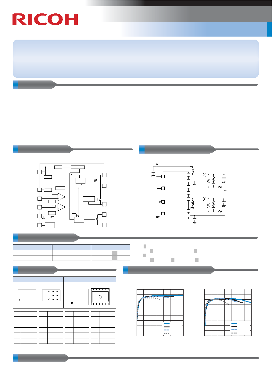
BLOCK DIAGRAM
TYPICAL APPLICATION
R1283x
LX1
VFB2
CE
LX2
VFB1
VREF
GND
VCC
PVCC
VOUTN
PGND
UVLO
Maxduty
Vref
Sequence
Control
Current Limit
PWM
Control
Timer
PWM
Control
Discharge
Control
R1283x00xB
VCC
CE
GND
VREF
VOUTN
VFB1
PGND
LX1
PVCC
VFB2
LX2
4.7
μF
"H"active
3.6V
SD
110k
Ω
1k
Ω
10
μF×2
VOUT1=12V
150pF
C5
10k
Ω
SD
75k
Ω
1k
Ω
10
μF
VOUT2=-7.5V
C6
12k
Ω
L2
6.8
μH
0.1
μF
L1
6.8
μH
150pF
SELECTION GUIDES
Package
Quantity per Reel
Part No.
WLCSP-11-P2
4,000 pcs
R1283Z00.
$ -E2-F
DFN(PLP)2730-12
5,000 pcs
R1283K00.
$ -TR
. : Select the start-up sequence from
(.1.) Step-up
→ Inverting or (.2.) Inverting → Step-up.
.$. : Select oscillator frequency from
(.A.) 300kHz, (.B.) 700kHz or (.C.) 1.4MHz.
PACKAGES
TYPICAL CHARACTERISTICS
WLCSP-11-P2
DFN(PLP)2730-12
R1283x001B Efficiency vs. Output Current
Bottom View
Top View
A
B
C
D
3
2
1
D
C
B
A
3
2
1
Bottom View
7
12
11
10
9
8
6
1
2
3
4
5
12
7
8
9
10
11
1
6
5
4
3
2
Top View
A1 PGND
A2 VFB1
A3 LX1
B1 PVCC
B2 CE
B3 LX2
C1 GND
C3 VOUTN
D1 VCC
D2 VREF
D3 VFB2
1
NC
2
LX1
3
LX2
4
VOUTN
5
CE
6
VFB2
7
VREF
8
VCC
9
VFB1
10 GND
11 PVCC
12 PGND
10
20
100
90
50
70
40
30
60
80
0
60
150 180
120
30
90
210
Output Current1 IOUT1(mA)
Efficiency
η
(%)
Topt=25°C, VOUT1=12V
VOUT2=-7.5V, IOUT2=0mA
VIN=5V
VIN=4.2V
VIN=3.6V
VIN=2.8V
10
20
100
90
50
70
40
30
60
80
0
80
200 240
160
40
120
280
Output Current2 IOUT2(mA)
Ef
ficiency
η
(%)
Topt=25°C, VOUT2=-7.5V
VOUT1=12V, IOUT1=0mA
VIN=5V
VIN=4.2V
VIN=3.6V
VIN=2.8V
) The tab is substrate level (GND).
APPLICATIONS
Power source for CCD, OLED and LCD
Power source for hand-held equipment
L1,L2 : VLF3010
SD : CRS02
相關(guān)PDF資料 |
PDF描述 |
|---|---|
| R1283Z1A-E2 | DC-DC REG PWR SUPPLY MODULE |
| R1285L591A | SWITCHING REGULATOR, 1600 kHz SWITCHING FREQ-MAX, DSO12 |
| R1285L273A | SWITCHING REGULATOR, 1600 kHz SWITCHING FREQ-MAX, DSO12 |
| R1285L311A | SWITCHING REGULATOR, 1600 kHz SWITCHING FREQ-MAX, DSO12 |
| R1285L462A | SWITCHING REGULATOR, 1600 kHz SWITCHING FREQ-MAX, DSO12 |
相關(guān)代理商/技術(shù)參數(shù) |
參數(shù)描述 |
|---|---|
| R128405161 | 功能描述:RF 連接器 EMB M DR P-FIT E C C100 RoHS:否 制造商:Bomar Interconnect 產(chǎn)品:Connectors 射頻系列:BNC 型式:Jack (Female) 極性: 觸點電鍍:Gold 阻抗: 端接類型:Solder 主體類型:Straight Bulkhead 電纜類型: |
| R128405161W | 功能描述:RF 連接器 EMB M DR P-FIT E C RoHS:否 制造商:Bomar Interconnect 產(chǎn)品:Connectors 射頻系列:BNC 型式:Jack (Female) 極性: 觸點電鍍:Gold 阻抗: 端接類型:Solder 主體類型:Straight Bulkhead 電纜類型: |
| R128414701 | 制造商:Radiall 功能描述:EMB PLAT CAR C50 - Bulk |
| R128424848 | 功能描述:RF 連接器 BMA(M) STR SMT RCPT RoHS:否 制造商:Bomar Interconnect 產(chǎn)品:Connectors 射頻系列:BNC 型式:Jack (Female) 極性: 觸點電鍍:Gold 阻抗: 端接類型:Solder 主體類型:Straight Bulkhead 電纜類型: |
| R128424848W | 功能描述:RF 連接器 EMB M DR CMS RoHS:否 制造商:Bomar Interconnect 產(chǎn)品:Connectors 射頻系列:BNC 型式:Jack (Female) 極性: 觸點電鍍:Gold 阻抗: 端接類型:Solder 主體類型:Straight Bulkhead 電纜類型: |
發(fā)布緊急采購,3分鐘左右您將得到回復(fù)。