- 您現(xiàn)在的位置:買(mǎi)賣(mài)IC網(wǎng) > PDF目錄373260 > REG1118-2.85 800mA Low Dropout Positive Regulator with Current Source and Sink Capability PDF資料下載
參數(shù)資料
| 型號(hào): | REG1118-2.85 |
| 英文描述: | 800mA Low Dropout Positive Regulator with Current Source and Sink Capability |
| 中文描述: | 800mA的低壓差穩(wěn)壓器的電流正源庫(kù)能力 |
| 文件頁(yè)數(shù): | 4/5頁(yè) |
| 文件大小: | 103K |
| 代理商: | REG1118-2.85 |
REG1118
4
APPLICATIONS INFORMATION
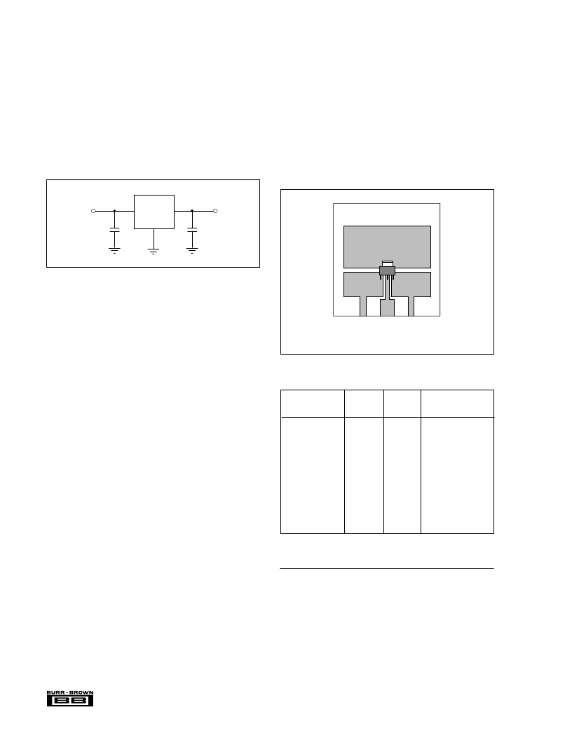
Figure 1 shows the basic hookup diagram for the REG1118.
An output capacitor is required for proper operation and to
improve high frequency load regulation. A high quality
capacitor should be used to assure that the ESR (effective
series resistance) is less than 0.5
. A capacitor of at least
1
μ
F is recommended. Increasing C
OUT
improves output
voltage deviation, see the typical curve “Load Transient
Response.” It is suggested that the input be decoupled with
10
μ
F low ESR capacitor.
ambient temperature above that expected in normal opera-
tion until the device’s thermal shutdown is activated. If this
occurs at more than 40
°
C above the maximum expected
ambient temperature, then the T
J
will be less than 125
°
C
during normal operation.
SOLDERING METHODS
The REG1118 package is suitable for infrared reflow and
vapor-phase reflow soldering techniques. The high rate of
temperature change that occurs with wave soldering, or hand
soldering can damage the REG1118.
FIGURE 1. Basic Connections.
THERMAL CONSIDERATIONS
The REG1118 has current limit and thermal shutdown
circuits that protect it from overload. The thermal shutdown
activates at approximately T
J
= 150
°
C. For continuous op-
eration, however, the junction temperature should not be
allowed to exceed 125
°
C. Any tendency to activate the
thermal shutdown in normal use is an indication of an
inadequate heat sink or excessive power dissipation. The
power dissipation is equal to:
P
D
= (V
IN
– V
OUT
) I
OUT
The junction temperature can be calculated by:
T
J
= T
A
+ P
D
(
θ
JA
)
where T
A
is the ambient temperature, and
θ
JA
is the junction-to-ambient thermal resistance
The REG1118 derives heat sinking from conduction through
its copper leads, especially the large mounting tab. These
must be soldered to a circuit board with a substantial amount
of copper remaining (see Figure 2). Circuit board traces
connecting to the tab and the leads should be made as large
as practical. Other nearby circuit traces, including those on
the back side of the circuit board, help conduct heat away
from the device, even though they are not electrically connected.
Make all nearby copper traces as wide as possible and leave
only narrow gaps between traces. In addition, multiple
contacts to internal power and ground planes increase heat
sinking with minimal increase in circuit board area.
Table I shows approximate values of
θ
JA
for various circuit
board and copper areas. Nearby heat dissipating compo-
nents, circuit board mounting conditions and ventilation can
dramatically affect the actual
θ
JA
.
A simple experiment will determine whether the maximum
recommended junction temperature is exceeded in an actual
circuit board and mounting configuration: Increase the
FIGURE 2. Circuit Board Layout Example.
Total Area: 50 x 50mm
Without back-side copper:
JA
≈
59°C/W
With solid back-side copper:
JA
≈
49°C/W
35 x 17 mm
16 x 10 mm
16 x 10 mm
θ
θ
TOPSIDE
(1)
COPPER
AREA
BACKSIDE
COPPER
AREA
TOTAL PC BOARD
AREA
THERMAL RESISTANCE
JUNCTION-TO-AMBIENT
46
°
C/W
47
°
C/W
49
°
C/W
51
°
C/W
53
°
C/W
55
°
C/W
58
°
C/W
59
°
C/W
67
°
C/W
72
°
C/W
85
°
C/W
2500mm
2
2500mm
2
2500mm
2
2500mm
2
1250mm
2
2500mm
2
2500mm
2
950mm
2
2500mm
2
2500mm
2
2500mm
2
0
2500mm
2
1800mm
2
0
1600mm
2
600mm
2
1600mm
2
2500mm
2
1250mm
2
0
2500mm
2
915mm
2
0
1600mm
2
600mm
2
0
900mm
2
340mm
2
900mm
2
900mm
2
340mm
2
0
NOTE: (1) Tab is attached to the topside copper.
TABLE I.
INSPEC Abstract Number: B91007604, C91012627
Kelly, E.G. “Thermal Characteristics of Surface 5WK9
Packages.” The Proceedings of SMTCON. Surface Mount
Technology Conference and Exposition:
Competitive Surface
Mount Technology
, April 3-6, 1990, Atlantic City, NJ, USA.
Abstract Publisher
: IC Manage, 1990, Chicago, IL, USA.
REG1118
V
O
V
IN
10μF
4.7μF
相關(guān)PDF資料 |
PDF描述 |
|---|---|
| REG1118 | 800mA Low Dropout Positive Regulator with Current Source and Sink Capability |
| REG710-25 | 30-mA Switched-Cap DC-DC Converter with fixed 2.5-V Output |
| REG710-27 | 30-mA Switched-Cap DC-DC Converter with fixed 2.7-V Output |
| REG710-3 | 30-mA Switched-Cap DC-DC Converter with fixed 3-V Output |
| REG710-33 | 30-mA Switched-Cap DC-DC Converter with fixed 3.3-V Output |
相關(guān)代理商/技術(shù)參數(shù) |
參數(shù)描述 |
|---|---|
| REG113 | 制造商:TI 制造商全稱(chēng):Texas Instruments 功能描述:DMOS 400mA Low-Dropout Regulator |
| REG113_07 | 制造商:TI 制造商全稱(chēng):Texas Instruments 功能描述:DMOS 400mA Low-Dropout Regulator |
| REG113_08 | 制造商:TI 制造商全稱(chēng):Texas Instruments 功能描述:DMOS 400mA Low-Dropout Regulator |
| REG113-25 | 制造商:未知廠家 制造商全稱(chēng):未知廠家 功能描述:DMOS 400mA Low-Dropout Regulator |
| REG113-285 | 制造商:未知廠家 制造商全稱(chēng):未知廠家 功能描述:DMOS 400mA Low-Dropout Regulator |
發(fā)布緊急采購(gòu),3分鐘左右您將得到回復(fù)。