- 您現(xiàn)在的位置:買賣IC網(wǎng) > PDF目錄373260 > REG113-285 DMOS 400mA Low-Dropout Regulator PDF資料下載
參數(shù)資料
| 型號(hào): | REG113-285 |
| 英文描述: | DMOS 400mA Low-Dropout Regulator |
| 中文描述: | 的DMOS 400mA的低壓差穩(wěn)壓器 |
| 文件頁數(shù): | 8/12頁 |
| 文件大小: | 382K |
| 代理商: | REG113-285 |
REG1117, REG1117A
SBVS001B
8
www.ti.com
The SOT-223 package derives heat sinking from conduction
through its copper leads, especially the large mounting tab.
These must be soldered to a circuit board with a substantial
amount of copper remaining, as shown in Figure 5. Circuit
board traces connecting the tab and the leads should be made
as large as practical. The mounting tab of both packages is
electrically connected to V
OUT
.
Without back-side copper:
θ
JA
≈
59
°
C/W
With solid back-side copper:
θ
JA
≈
49
°
C/W
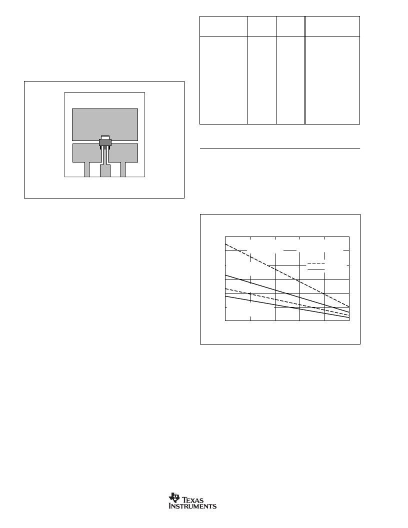
FIGURE 5. SOT-223 Circuit Board Layout Example.
Other nearby circuit traces, including those on the back side
of the circuit board, help conduct heat away from the device,
even though they may not be electrically connected. Make
all nearby copper traces as wide as possible and leave only
narrow gaps between traces.
Table I shows approximate values of
θ
JA
for various circuit
board and copper areas for the SOT-223 package. Nearby
heat dissipating components, circuit board mounting condi-
tions, and ventilation can dramatically affect the actual
θ
JA
.
Proper heat sinking significantly increases the maximum
power dissipation at a given ambient temperature, as shown
in Figure 6.
SOLDERING METHODS
Both REG1117 packages are suitable for infrared reflow and
vapor-phase reflow soldering techniques. The high rate of
temperature change that occurs with wave soldering, or hand
soldering can damage the REG1117.
TOPSIDE
(1)
COPPER
AREA
BACKSIDE
COPPER
AREA
SOT-223
TOTAL PC BOARD
AREA
THERMAL RESISTANCE
JUNCTION-TO-AMBIENT
46
°
C/W
47
°
C/W
49
°
C/W
51
°
C/W
53
°
C/W
55
°
C/W
58
°
C/W
59
°
C/W
67
°
C/W
72
°
C/W
85
°
C/W
2500mm
2
2500mm
2
2500mm
2
2500mm
2
1250mm
2
2500mm
2
2500mm
2
950mm
2
2500mm
2
2500mm
2
2500mm
2
0
2500mm
2
1800mm
2
0
1600mm
2
600mm
2
1600mm
2
2500mm
2
1250mm
2
0
2500mm
2
915mm
2
0
1600mm
2
600mm
2
0
900mm
2
340mm
2
900mm
2
900mm
2
340mm
2
0
NOTE: (1) Tab is attached to the topside copper.
TABLE I.
INSPEC Abstract Number: B91007604, C91012627
Kelly, E.G. “Thermal Characteristics of Surface 5WK9
Packages.” The Proceedings of SMTCON. Surface Mount
Technology Conference and Exposition:
Competitive Surface
Mount Technology
, April 3-6, 1990, Atlantic City, NJ, USA.
Abstract Publisher
: IC Manage, 1990, Chicago, IL, USA.
FIGURE 6. Maximum Power Dissipation versus Ambient
Temperature.
Total Area: 50 x 50mm
35 x 17 mm
16 x 10 mm
16 x 10 mm
6
5
4
3
2
1
0
P
0
25
50
75
100
125
Ambient Temperature (
°
C)
MAXIMUM POWER DISSIPATION
vs AMBIENT TEMPERATURE
P
D
= (T
(max)
–
T
A
)
/
JA
T
J
(max) = 150
°
C
θ
DDPAK
SOT-223
= 85
°
C/W
(340mm
2
topside copper,
no backside copper)
θ
= 46
°
C/W
(2500mm
2
topside and
backside copper)
θ
= 27
°
C/W
(4in
one oz copper
mounting pad)
θ
θ
= 65
°
C/W
(no heat sink)
相關(guān)PDF資料 |
PDF描述 |
|---|---|
| REG113-3 | DMOS 400mA Low-Dropout Regulator |
| REG113-33 | DMOS 400mA Low-Dropout Regulator |
| REG113-5 | DMOS 400mA Low-Dropout Regulator |
| REG1117FA-5 | THREE-TERMINAL POSITIVE FIXED VOLTAGE REGULATORS |
| REG1117FA-TR | Positive Adjustable Voltage Regulator |
相關(guān)代理商/技術(shù)參數(shù) |
參數(shù)描述 |
|---|---|
| REG113-3 | 制造商:未知廠家 制造商全稱:未知廠家 功能描述:DMOS 400mA Low-Dropout Regulator |
| REG113-33 | 制造商:未知廠家 制造商全稱:未知廠家 功能描述:DMOS 400mA Low-Dropout Regulator |
| REG113-5 | 制造商:未知廠家 制造商全稱:未知廠家 功能描述:DMOS 400mA Low-Dropout Regulator |
| REG113EA-2.5/250 | 功能描述:低壓差穩(wěn)壓器 - LDO DMOS 400mA Regulator Low-Dropout RoHS:否 制造商:Texas Instruments 最大輸入電壓:36 V 輸出電壓:1.4 V to 20.5 V 回動(dòng)電壓(最大值):307 mV 輸出電流:1 A 負(fù)載調(diào)節(jié):0.3 % 輸出端數(shù)量: 輸出類型:Fixed 最大工作溫度:+ 125 C 安裝風(fēng)格:SMD/SMT 封裝 / 箱體:VQFN-20 |
| REG113EA-2.5/250G4 | 功能描述:低壓差穩(wěn)壓器 - LDO DMOS 400mA Regulator Low-Dropout RoHS:否 制造商:Texas Instruments 最大輸入電壓:36 V 輸出電壓:1.4 V to 20.5 V 回動(dòng)電壓(最大值):307 mV 輸出電流:1 A 負(fù)載調(diào)節(jié):0.3 % 輸出端數(shù)量: 輸出類型:Fixed 最大工作溫度:+ 125 C 安裝風(fēng)格:SMD/SMT 封裝 / 箱體:VQFN-20 |
發(fā)布緊急采購(gòu),3分鐘左右您將得到回復(fù)。