- 您現(xiàn)在的位置:買賣IC網(wǎng) > PDF目錄373261 > RF1046 Analog IC PDF資料下載
參數(shù)資料
| 型號: | RF1046 |
| 英文描述: | Analog IC |
| 中文描述: | 模擬IC |
| 文件頁數(shù): | 1/3頁 |
| 文件大小: | 100K |
| 代理商: | RF1046 |
RF1046 1333 MHz SAW Filter
RF Monolithics, Inc.
4347 Sigma Road
Dallas, Texas 75244
USA
Phone: +1(972)233-2903
Fax: +1(972)387-8148
e-mail:
info@rfm.com
Home page:
www.rfm.com
European Sales Office
RF1046 7/22/1999 R
Electrical Connections
(See note 3)
Connection
Port 1 Hot
Port 2 Hot
Case Ground
Terminals
1 (near tab)
2
3
Absolute Maximum Ratings
Rating
Maximum Incident Power in Passband
Max. DC voltage between any 2 terminals
Storage Temperature Range
Max Soldering Profile
Value
+10
30
-55 to +85
265
°
C for 10 s
Units
dBm
VDC
°
C
Designed for Front-End of RF Detector
Simple External Impedance Matching
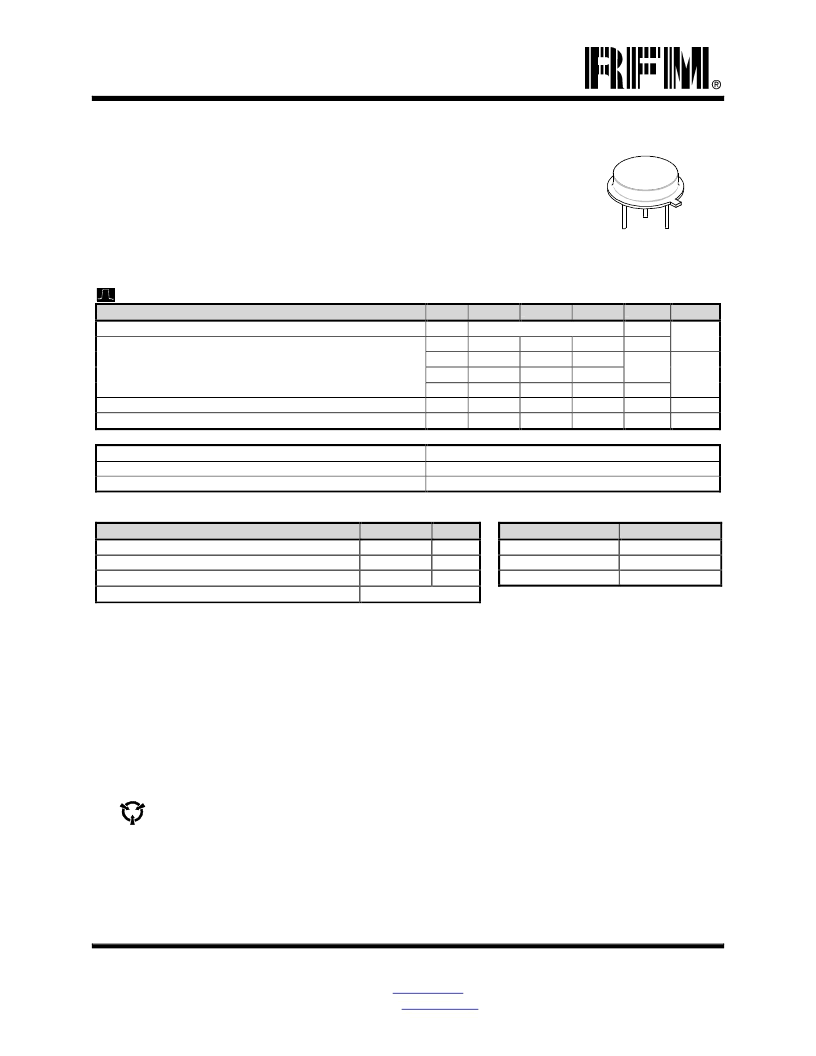
Hermetic TO39-3 Case
Unbalanced Input and Output
See Associated Plots
Characteristic
Nominal Center Frequency
Passband
Sym
fc
IL
BW
1
BW
3
Min
Typ
Max
Units
MHz
dB
kHz
Notes
1
1333.000
6
8.0
±
175
±
850
200
63
Insertion Loss at fc
1 dB Passband
3 dB Passband
Group Delay Variation over fc
±
175 kHz GDV
< fc-140 MHz and > fc+140 MHz
Operating Temperature Range
1000
ns
P-P
dB
°
C
1, 2
Rejection
55
-55
1, 2, 3
1
T
A
+85
Impedance Matching to 50
unbalanced
Case Style
Lid Symbolization
External L-C
TO39-3 9.3 mm Diameter Nominal Footprint
RFM RF1046 Lot-Code
Notes:
1.
Unless noted otherwise, all specifications apply
over the operating temperature range
with filter soldered to the specified
demonstration board with impedance matching to 50
and measured with 50
network analyzer.
Unless noted otherwise, all frequency specifications are referenced to the nominal center frequency, fc.
Rejection is measured as attenuation below the minimum IL point in the passband. Rejection in final user application is dependent
on PCB layout and external impedance matching design. See Application Note No. 42 for details. All “NC” or “no connection”
terminals should be grounded.
“LRIP” or “L” after the part number indicates “l(fā)ow rate initial production” and “ENG” or “E” indicates “engineering prototypes.”
The design, manufacturing process, and specifications of this filter are subject to change.
Either Port 1 or Port 2 may be used for either input or output in the design. However, impedances and impedance matching may
vary between Port 1 and Port 2, so that the filter must always be installed in one direction per the circuit design.
US and international patents may apply.
RFM, stylized RFM logo, and RF Monolithics, Inc. are registered trademarks of RF Monolithics, Inc.
Copyright 1999, RF Monolithics Inc.
10. Electrostatic Sensitive Device. Observe precautions for handling.
2.
3.
4.
5.
6.
7.
8.
9.
相關PDF資料 |
PDF描述 |
|---|---|
| RF105 | 900 MHz Digital Spread Spectrum Transceiver |
| RF110 | 2400 MHz Power Amplifier |
| RF1171 | Analog IC |
| RF1171B | Analog IC |
| RF1172-2 | Analog IC |
相關代理商/技術參數(shù) |
參數(shù)描述 |
|---|---|
| RF1046-000 | 制造商:TE Connectivity 功能描述:PTC Resettable Fuse 100A 32VDC Bulk 制造商:TE Connectivity 功能描述:AHEF100 - Bag 制造商:TE Connectivity 功能描述:POLYSWITCH PTC RESET 1.0A HOLD 制造商:TE CONNECTIVITY RAYCHEM-POLYSWITCH 功能描述:RLINE / AHEF100 |
| RF104J250V | 制造商:IMP 功能描述:RF410X250V .4 IMP 5% |
| RF104K100 | 制造商:CAP 功能描述:RF410X100 CAPAR |
| RF104K50V | 制造商:ILL CAP 功能描述:RF410X050 |
| RF1-04-T-01-75 | 制造商:ADAM-TECH 制造商全稱:Adam Technologies, Inc. 功能描述:RF CONNECTORS BNC STYLE |
發(fā)布緊急采購,3分鐘左右您將得到回復。