- 您現(xiàn)在的位置:買賣IC網(wǎng) > PDF目錄385768 > RF2318PCBA-L (RF Micro Devices, Inc.) LINEAR BROADBAND AMPLIFIER PDF資料下載
參數(shù)資料
| 型號: | RF2318PCBA-L |
| 廠商: | RF Micro Devices, Inc. |
| 英文描述: | LINEAR BROADBAND AMPLIFIER |
| 中文描述: | 線性寬帶放大器 |
| 文件頁數(shù): | 4/6頁 |
| 文件大小: | 110K |
| 代理商: | RF2318PCBA-L |
Preliminary
3-24
RF2318
Rev A2 010228
3
L
A
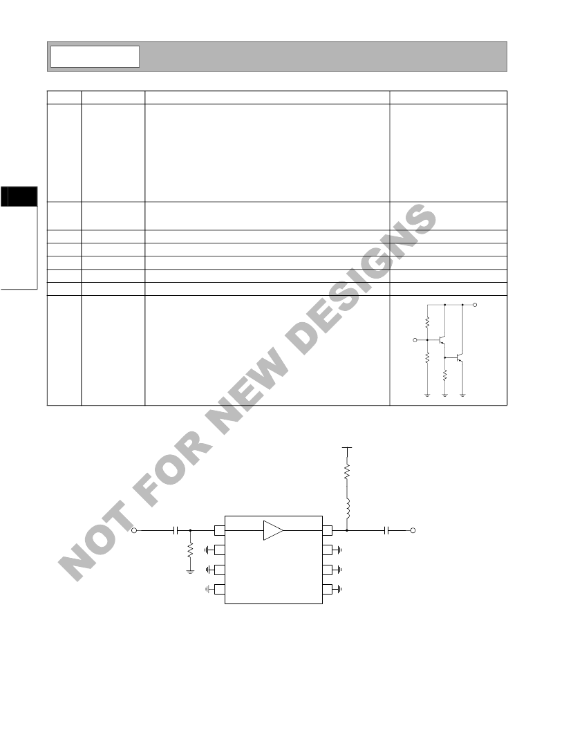
Application S chematic
Pin
1
Function
RF IN
Description
RF input pin. This pin is NOT internally DC blocked. A DC blocking
capacitor, suitable for the frequency of operation, should be used in all
applications. The device has internal feedback, and not using a DC
blocking capacitor will disable the temperature compensation.The bias
of the device can be controlled by this pin. Adding an optional 1k
resistor to ground on this pin reduces the bias level, which may be com-
pensated for by a higher supply voltage to maintain the appropriate
bias level. The net effect of this is an increased output power capability,
as well as higher linearity for signals with high crest factors. DC cou-
pling of the input is not allowed, because this will override the internal
feedback loop and cause temperature instability.
Ground connection. Keep traces physically short and connect immedi-
ately to ground plane for best performance. Each ground pin should
have a via to the ground plane.
Same as pin 2.
Interface Schematic
2
GND
3
4
5
6
7
8
GND
GND
GND
GND
GND
RF OUT
Same as pin 2.
Same as pin 2.
Same as pin 2.
Same as pin 2.
RF output and bias pin. Because DC is present on this pin, a DC block-
ing capacitor, suitable for the frequency of operation, should be used in
most applications. For biasing, an RF choke in series with a resistor is
needed. The value for the resistor R
C
is 30
(0.5W) for V
CC
=9V and
82
for V
CC
=12V. The DC voltage on this pin is typically 7V with a cur-
rent of 63mA. In lower power applications the value of R
C
can be
increased to lower the current and V
D
on this pin.
RF OUT
RF IN
1
2
3
4
8
7
6
5
220 pF
RF OUT
220 pF
RF IN
3.3
μ
H
R
C
= 30 - 82
V
CC
= 9 - 12 V
Optional:
R
=1 - 2 k
Note 1
Note 1:
Optional resistor Rs can be used to maintain the correct bias level at higher supply voltages. This
is useful to increase output capability or linearity for signals with high crest factors.
相關(guān)PDF資料 |
PDF描述 |
|---|---|
| RF2318 | LINEAR BROADBAND AMPLIFIER |
| RF2321PCBA | 3V GENERAL PURPOSE AMPLIFIER |
| RF2321 | 3V GENERAL PURPOSE AMPLIFIER |
| RF2326PCBA | 3V GENERAL PURPOSE AMPLIFIER |
| RF2326 | 3V GENERAL PURPOSE AMPLIFIER |
相關(guān)代理商/技術(shù)參數(shù) |
參數(shù)描述 |
|---|---|
| RF2319 | 制造商:未知廠家 制造商全稱:未知廠家 功能描述:Analog IC |
| RF2320 | 制造商:RFMD 制造商全稱:RF Micro Devices 功能描述:LINEAR GENERAL PURPOSE AMPLIFIER |
| RF2320_07 | 制造商:RFMD 制造商全稱:RF Micro Devices 功能描述:LINEAR GENERAL PURPOSE AMPLIFIER |
| RF2320PCBA | 制造商:RFMD 制造商全稱:RF Micro Devices 功能描述:LINEAR GENERAL PURPOSE AMPLIFIER |
| RF2320PCBA-41X | 制造商:RFMD 制造商全稱:RF Micro Devices 功能描述:LINEAR GENERAL PURPOSE AMPLIFIER |
發(fā)布緊急采購,3分鐘左右您將得到回復(fù)。