- 您現(xiàn)在的位置:買賣IC網(wǎng) > PDF目錄385768 > RF2352 (RF MICRO DEVICES INC) 3V CDMA DRIVER AMPLIFIER PDF資料下載
參數(shù)資料
| 型號: | RF2352 |
| 廠商: | RF MICRO DEVICES INC |
| 元件分類: | 衰減器 |
| 英文描述: | 3V CDMA DRIVER AMPLIFIER |
| 中文描述: | 824 MHz - 925 MHz RF/MICROWAVE WIDE BAND LOW POWER AMPLIFIER |
| 封裝: | 4 X 4 MM, LCC, QFN-16 |
| 文件頁數(shù): | 3/6頁 |
| 文件大小: | 77K |
| 代理商: | RF2352 |
Preliminary
4-179
RF2352
Rev A4 010720
4
G
A
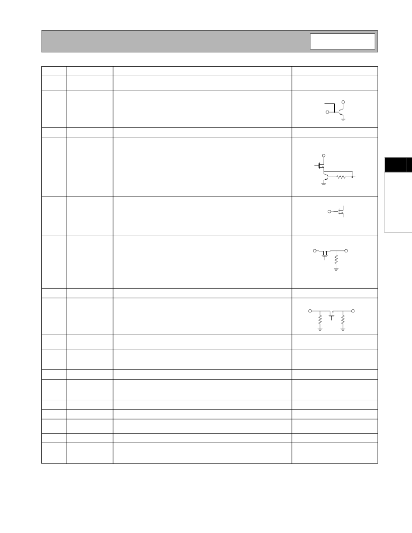
Pin
1
Function
GND
Description
Ground connection. For best performance, keep traces physically short
and connect immediately to ground plane.
RF input pin. It is DC-coupled and looks like 50
from 824MHz to
925MHz.
Interface Schematic
2
RF IN
3
4
NC
VREF
Not connected.
Provides the bias voltage for controlling the RF amplifier current drain.
This pin is typically connected through a resistor to an external regu-
lated power supply. It may be connected to the same power supply as
the VCC pin. However, if more bias control is desired, it may be con-
nected to a separate supply. With a series external resistor of 1500
and power supply of 3V applied, the amplifier current drain should be
around 14mA. By increasing the resistor, the amplifier current drain
may be dropped. Conversely, by decreasing the resistor, the amplifier
current may be increased to a maximum of 30mA.
Power down function. When 0V to 0.5V is applied, the device is in
Bypass Mode: the amplifier is shut off and the MOSFET switches are
activated. There is no DC current dissipation in this state. When 1.5V to
3V is applied, the device is switched to High Gain Mode: the amplifier is
activated and the MOSFET switches are opened. This is the normal
operating mode.
Output of the first MOSFET switch. DC-coupled. When the PD pin is
grounded (Bypass Mode), the MOSFET switches are shorted, sending
any signals at the RF IN pin through the first MOSFET and off the chip.
In cases where minimum RF attenuation is desired, this pin should be
shorted with 50
microstrip to the ATT IN pin. This setup will yield
approximately 4dB of insertion loss. If more attenuation is desired, a
resistive pad between the ATT OUT1 and ATT IN pins can be added to
the PC board.
Not connected.
5
PD
6
ATT OUT1
7
8
NC
ATT IN
Input to the second MOSFET switch. DC-coupled. When the PD pin is
grounded (Bypass Mode), the MOSFET switches are shorted. See the
ATT OUT1 pin description for setup options.
9
GND
Ground connection. For best performance, keep traces physically short
and connect immediately to ground plane.
Output of the second MOSFET switch. DC-coupled. When the PD pin
is grounded (Bypass Mode), the MOSFET switches are shorted. This
pin should be shorted with 50
microstrip to the amplifier load.
Provides the power supply to the logic circuitry on the IC.
10
ATT OUT2
11
12
VCC
RF OUT
Amplifier output pin. An open collector output that needs VCC applied
to it through an inductor. Typically, a shunt inductor, series capacitor
matching network is used to provide a 50
output match.
Not connected.
13
14
15
NC
NC
Not connected.
RF GND
Amplifier ground. For best performance, keep traces physically short
and connect immediately to ground plane.
Not connected.
16
Pkg
Base
NC
GND
Ground connection for die flag. The backside of the package should be
soldered to a top side ground pad which is connected to the ground
plane with multiple vias.
RF OUT
RF IN
Bias
VREF
PD
RF IN
ATT OUT1
ATT OUT2
ATT IN
相關(guān)PDF資料 |
PDF描述 |
|---|---|
| RF2352PCBA | 3V CDMA DRIVER AMPLIFIER |
| RF2360 | LINEAR GENERAL PURPOSE AMPLIFIER |
| RF2360411 | LINEAR GENERAL PURPOSE AMPLIFIER |
| RF2360412 | LINEAR GENERAL PURPOSE AMPLIFIER |
| RF2360PCBA | LINEAR GENERAL PURPOSE AMPLIFIER |
相關(guān)代理商/技術(shù)參數(shù) |
參數(shù)描述 |
|---|---|
| RF2352PCBA | 制造商:RFMD 制造商全稱:RF Micro Devices 功能描述:3V CDMA DRIVER AMPLIFIER |
| RF2360 | 制造商:RFMD 制造商全稱:RF Micro Devices 功能描述:LINEAR GENERAL PURPOSE AMPLIFIER |
| RF2360_06 | 制造商:RFMD 制造商全稱:RF Micro Devices 功能描述:LINEAR GENERAL PURPOSE AMPLIFIER |
| RF2360_1 | 制造商:RFMD 制造商全稱:RF Micro Devices 功能描述:LINEAR GENERAL PURPOSE AMPLIFIER |
| RF2360411 | 制造商:RFMD 制造商全稱:RF Micro Devices 功能描述:LINEAR GENERAL PURPOSE AMPLIFIER |
發(fā)布緊急采購,3分鐘左右您將得到回復(fù)。