- 您現(xiàn)在的位置:買(mǎi)賣(mài)IC網(wǎng) > PDF目錄373262 > RF2412 RF Modulator PDF資料下載
參數(shù)資料
| 型號(hào): | RF2412 |
| 英文描述: | RF Modulator |
| 中文描述: | 射頻調(diào)制器 |
| 文件頁(yè)數(shù): | 3/8頁(yè) |
| 文件大?。?/td> | 124K |
| 代理商: | RF2412 |
9-3
RF2410
Rev B1 010329
9
A
S
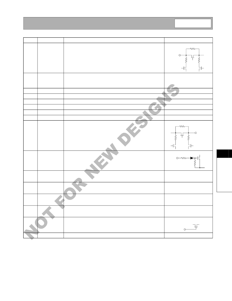
Pin
1
Function
RF IN
Description
RF Input. This pin is not DC blocked, and an external blocking capacitor
is recommended. The value depends on the frequency used.
Interface Schematic
2
GND
Ground connection. Keep traces physically short and connect immedi-
ately to the ground plane for best performance. Each ground pin should
be connected to the ground plane individually, rather than using one
trace and/or via for all ground pins. This will give better step accuracy.
Same as pin 2.
3
4
5
6
7
8
9
GND
GND
GND
GND
GND
GND
RF OUT
Same as pin 2.
Same as pin 2.
Same as pin 2.
Same as pin 2.
Same as pin 2.
RF Output. This pin is not DC blocked, and an external blocking capac-
itor is recommended. The value depends on the frequency used.
10
G16
Control pin for the 16dB attenuator. This pin has an internal pull-down
resistor, so when the pin is not connected the attenuator will be turned
off. For operating frequencies above 1GHz this bit should always be left
"off".
11
G8B
Control pin for the 8dB attenuator. This pin has an internal pull-down
resistor, so when the pin is not connected the attenuator will be turned
off.
Control pin for the 8dB attenuator. This pin has an internal pull-down
resistor, so when the pin is not connected the attenuator will be turned
off.
Control pin for the 4dB attenuator. This pin has an internal pull-down
resistor, so when the pin is not connected the attenuator will be turned
off.
Control pin for the 2dB attenuator. This pin has an internal pull-down
resistor, so when the pin is not connected the attenuator will be turned
off.
Power Down control pin. This pin has an internal pull-up resistor to
VDD of 10k
. When this pin is "low" the circuits are turned off. A "low"
means as close to 0V as possible, to ensure minimum current con-
sumption when turned off.
Power supply pin. An external RF bypass capacitor is recommended.
Same as pin 10.
12
G8A
Same as pin 10.
13
G4
Same as pin 10.
14
G2
Same as pin 10.
15
PD
16
VDD
RF IN
RF OUT
Gxx
PD
相關(guān)PDF資料 |
PDF描述 |
|---|---|
| RF2431 | RF Mixer |
| RF2450 | Analog IC |
| RF2454 | RF Modulator |
| RF2464 | RF Modulator |
| RF24 | Analog IC |
相關(guān)代理商/技術(shù)參數(shù) |
參數(shù)描述 |
|---|---|
| RF-2412D | 制造商:RECOM 制造商全稱(chēng):Recom International Power 功能描述:ECONOLINE - DC/DC - CONVERTER |
| RF-2412DH | 制造商:RECOM 制造商全稱(chēng):Recom International Power 功能描述:ECONOLINE - DC/DC - CONVERTER |
| RF-2412S | 制造商:RECOM 制造商全稱(chēng):Recom International Power 功能描述:ECONOLINE - DC/DC - CONVERTER |
| RF-2412SH | 制造商:RECOM 制造商全稱(chēng):Recom International Power 功能描述:ECONOLINE - DC/DC - CONVERTER |
| RF2413 | 制造商:RFMD 制造商全稱(chēng):RF Micro Devices 功能描述:GAIN CONTROLLED DUAL-CONVERSION QUADRATURE MODULATOR |
發(fā)布緊急采購(gòu),3分鐘左右您將得到回復(fù)。