- 您現(xiàn)在的位置:買賣IC網(wǎng) > PDF目錄385768 > RF2420PCBA (RF Micro Devices, Inc.) PROGRAMMABLE ATTENUATOR PDF資料下載
參數(shù)資料
| 型號: | RF2420PCBA |
| 廠商: | RF Micro Devices, Inc. |
| 英文描述: | PROGRAMMABLE ATTENUATOR |
| 中文描述: | 可編程衰減器 |
| 文件頁數(shù): | 3/6頁 |
| 文件大小: | 61K |
| 代理商: | RF2420PCBA |
9-11
RF2420
Rev A6 010720
9
A
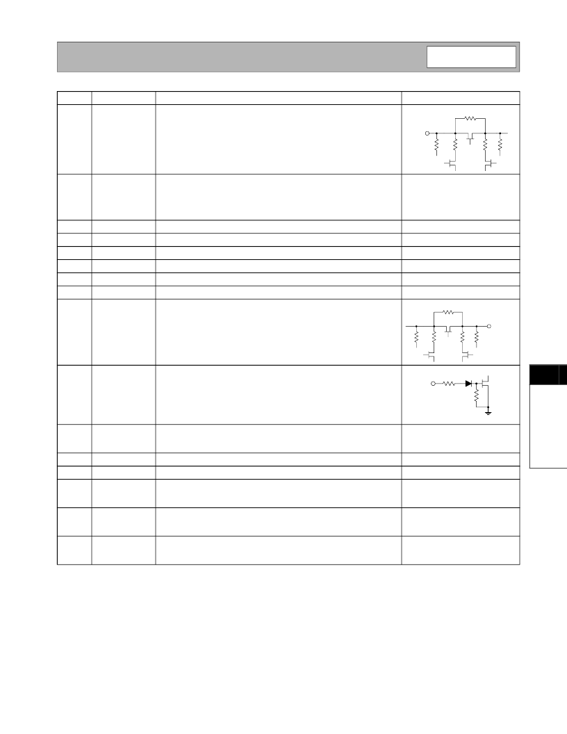
S
Pin
1
Function
RF IN
Description
RF Input. This pin is not DC-blocked, and an external blocking capaci-
tor is required. The value depends on the frequency used. The DC
value on this pin is approximately equal to VDD.
Interface Schematic
2
VDD
VDD supply connection. Bypassing is critical: To achieve maximum
attenuation range the magnitude of the impedance at the operation fre-
quency, as seen from the package pins, needs to be less than 0.5
.
The DC source to the pin may be a logic driver gate to implement a
Power Down function.
Same as pin 2.
3
4
5
6
7
8
9
VDD
VDD
VDD
VDD
VDD
VDD
RF OUT
Same as pin 2.
Same as pin 2.
Same as pin 2.
Same as pin 2.
Same as pin 2.
RF Output. Same as pin 1. Pin 1 and 9 are interchangeable.
10
G20
Control pin for the 20dB attenuator. This pin has an internal pull-down
resistor, so when the pin is not connected the attenuator will be turned
off.
11
G10
Control pin for the 10dB attenuator. This pin has an internal pull-down
resistor, so when the pin is not connected the attenuator will be turned
off.
Ground.
Same as pin 10.
12
13
14
GND
GND
G8
Ground.
Control pin for the 8dB attenuator. This pin has an internal pull-down
resistor, so when the pin is not connected the attenuator will be turned
off.
Control pin for the 4dB attenuator. This pin has an internal pull-down
resistor, so when the pin is not connected the attenuator will be turned
off.
Control pin for the 2dB attenuator. This pin has an internal pull-down
resistor, so when the pin is not connected the attenuator will be turned
off.
Same as pin 10.
15
G4
Same as pin 10.
16
G2
Same as pin 10.
RF IN
RF OUT
Gxx
相關(guān)PDF資料 |
PDF描述 |
|---|---|
| RF2420 | PROGRAMMABLE ATTENUATOR |
| RF2421PCBA | 10dB SWITCHED ATTENUATOR |
| RF2421 | 10dB SWITCHED ATTENUATOR |
| RF2422 | 2.5GHZ DIRECT QUADRATURE MODULATOR |
| RF2422PCBA | 2.5GHZ DIRECT QUADRATURE MODULATOR |
相關(guān)代理商/技術(shù)參數(shù) |
參數(shù)描述 |
|---|---|
| RF2421 | 制造商:RFMD 制造商全稱:RF Micro Devices 功能描述:10dB SWITCHED ATTENUATOR |
| RF2421PCBA | 制造商:RFMD 制造商全稱:RF Micro Devices 功能描述:10dB SWITCHED ATTENUATOR |
| RF2422 | 制造商:RFMD 制造商全稱:RF Micro Devices 功能描述:2.5GHZ DIRECT QUADRATURE MODULATOR |
| RF2422_06 | 制造商:RFMD 制造商全稱:RF Micro Devices 功能描述:2.5GHZ DIRECT QUADRATURE MODULATOR |
| RF2422_1 | 制造商:RFMD 制造商全稱:RF Micro Devices 功能描述:2.5GHZ DIRECT QUADRATURE MODULATOR |
發(fā)布緊急采購,3分鐘左右您將得到回復(fù)。